


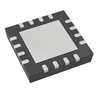
MD1812K6-G
ActiveHIGH SPEED QUAD MOSFET DRIVER 16 QFN 4X4X0.9MM T/R ROHS COMPLIANT: YES

MD1812K6-G
ActiveHIGH SPEED QUAD MOSFET DRIVER 16 QFN 4X4X0.9MM T/R ROHS COMPLIANT: YES
Description
General part information
MD1812 Series
MD1812 is a high-speed quad MOSFET driver. It is designed to drive two N and two P-channel high voltage DMOS FETs for medical ultrasound applications, but may be used in any application that needs a high output current for a capacitive load. The input stage of the MD1812 is a high-speed level translator that is able to operate from logic input signals of 1.8 to 5.0V amplitude. An adaptive threshold circuit is used to set the level translator threshold to the average of the input logic 0 and logic 1 levels. The level translator uses a proprietary circuit which provides DC coupling together with high-speed operation. The output stage of the MD1812 has separate power connections enabling the output signal L and H levels to be chosen independently from the driver supply voltages.
As an example, the input logic levels may be 0V and 1.8V, the control logic may be powered by +5V and –5V, and the output L and H levels may be varied anywhere over the range of -5.0 to +5.0V. The output stage is capable of peak currents of up to ±2.0 amps depending on the supply voltages used and load capacitance. The OE pin serves a dual purpose. First, its logic H level is used to compute the threshold voltage level for the channel input level translators. Secondly, when OE is low, the outputs are disabled, with the A and C outputs high and the B and D outputs low. This assists in properly pre-charging the coupling capacitors that may be used in series in the gate drive circuit of an external PMOS and NMOS. A built-in level shifter provides PMOS gate negative bias drive. This enables the user-defined damping control to generate return-to-zero bipolar output pulses.
Technical Specifications
Parameters and characteristics for this part
| Specification | MD1812K6-G |
|---|---|
| Channel Type | Independent |
| Current - Peak Output (Sink) | 2 A |
| Current - Peak Output (Source) | 2 A |
| Driven Configuration | Half-Bridge |
| Fall Time (Typ) | 6 ns |
| Gate Channel | N-Channel, P-Channel |
| Gate Type | N-Channel, P-Channel MOSFET, MOSFET |
| Input Type | Inverting |
| Logic Voltage - VIH | 1.7 V |
| Logic Voltage - VIL | 0.3 V |
| Mounting Type | Surface Mount |
| Number of Drivers | 4 |
| Operating Temperature (Max) | 125 °C |
| Operating Temperature (Min) | -25 °C |
| Package / Case | 16-VQFN Exposed Pad |
| Package Length | 4 mm |
| Package Name | 16-QFN |
| Package Width | 4 mm |
| Rise Time (Typ) | 6 ns |
| Voltage - Supply (Maximum) | 13 V |
| Voltage - Supply (Minimum) | 4.5 V |
Pricing
Prices provided here are for design reference only. For realtime values and availability, please visit the distributors directly
Sign in to see pricing
Create a free account to access distributor pricing data.
CAD
3D models and CAD resources for this part
Documents
Technical documentation and resources