


874S02BMILF
ObsoleteDIFFERENTIAL-TO-LVDS ZERO DELAY CLOCK GENERATOR

874S02BMILF
ObsoleteDIFFERENTIAL-TO-LVDS ZERO DELAY CLOCK GENERATOR
Description
General part information
874S02I Series
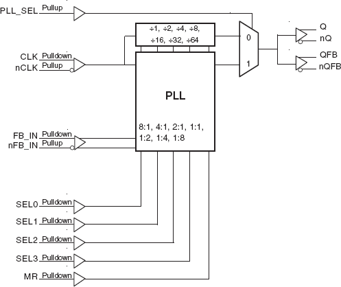
The 874S02I is a highly versatile 1:1 Differential-to-LVDS Clock Generator and a member of the family of High Performance Clock Solutions from IDT. The 874S02I has a fully integrated PLL and can be configured as a zero delay buffer, multiplier or divider, and has an output frequency range of 62.5MHz to 1GHz. The reference divider, feedback divider and output divider are each programmable, thereby allowing for the following output-to-input frequency ratios: 8:1, 4:1, 2:1, 1:1, 1:2, 1:4, 1:8. The external feedback allows the device to achieve "zero delay" between the input clock and the output clocks. The PLL_SEL pin can be used to bypass the PLL for system test and debug purposes. In bypass mode, the reference clock is routed around the PLL and into the internal output dividers.
Technical Specifications
Parameters and characteristics for this part
| Specification | 874S02BMILF |
|---|---|
| Differential Input | Yes |
| Differential Output | Yes |
| Divider | Yes |
| Frequency - Max | 1 GHz |
| Input | LVHSTL, SSTL, LVDS, LVPECL |
| Input Ratio | 1 |
| Mounting Type | Surface Mount |
| Multiplier | Yes |
| Number of Circuits | 1 |
| Operating Temperature (Max) | 85 °C |
| Operating Temperature (Min) | -40 °C |
| Output | LVDS |
| Output Ratio | 2 |
| Package Length | 0.295 in |
| Package Name | 20-SOIC |
| Package Width | 7.5 mm |
| PLL | Yes with Bypass |
| Voltage - Supply (Maximum) | 3.465 V |
| Voltage - Supply (Minimum) | 3.135 V |
Pricing
Prices provided here are for design reference only. For realtime values and availability, please visit the distributors directly
Sign in to see pricing
Create a free account to access distributor pricing data.
CAD
3D models and CAD resources for this part
Documents
Technical documentation and resources