SN74LVC16373ADGVR
ActiveTexas Instruments
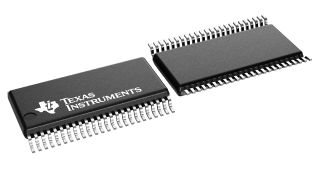
16-BIT TRANSPARENT D-TYPE LATCH WITH 3-STATE OUTPUTS 48-TVSOP -40 TO 125
Deep-Dive with AI
Search across all available documentation for this part.
SN74LVC16373ADGVR
ActiveTexas Instruments
16-BIT TRANSPARENT D-TYPE LATCH WITH 3-STATE OUTPUTS 48-TVSOP -40 TO 125
Deep-Dive with AI
Technical Specifications
Parameters and characteristics commom to parts in this series
| Specification | SN74LVC16373ADGVR | 74LVC16373 Series |
|---|---|---|
| Circuit | 8:8 | 8:8 |
| Current - Output High, Low [custom] | 24 mA | 24 mA |
| Current - Output High, Low [custom] | 24 mA | 24 mA |
| Delay Time - Propagation | 2.1 ns | 1.3 - 8 ns |
| Independent Circuits | 2 | 1 - 2 |
| Logic Type | D-Type Transparent Latch | D-Type Transparent Latch |
| Mounting Type | Surface Mount | Surface Mount |
| Operating Temperature [Max] | 85 °C | 85 - 125 °C |
| Operating Temperature [Min] | -40 °C | -55 - -40 °C |
| Output Type | Tri-State | Tri-State, Tri-State, Non-Inverted |
| Package / Case | 48-TFSOP | 48-BSSOP (0.295", 7.50mm Width), 48-TFSOP, 56-VFBGA |
| Package / Case | - | 6.1 mm |
| Package / Case | - | 0.24 in |
| Supplier Device Package | - | 48-SSOP, 48-TSSOP, 56-BGA Microstar Junior (7x4.5) |
| Voltage - Supply [Max] | 3.6 V | 3.6 V |
| Voltage - Supply [Min] | 1.65 V | 1.65 V |
Pricing
Prices provided here are for design reference only. For realtime values and availability, please visit the distributors directly
74LVC16373 Series
16-BIT TRANSPARENT D-TYPE LATCH WITH 3-STATE OUTPUTS 48-SSOP -40 TO 125
| Part | Circuit | Package / Case | Logic Type | Independent Circuits | Operating Temperature [Min] | Operating Temperature [Max] | Supplier Device Package | Output Type | Voltage - Supply [Max] | Voltage - Supply [Min] | Delay Time - Propagation | Current - Output High, Low [custom] | Current - Output High, Low [custom] | Mounting Type | Package / Case [y] | Package / Case |
|---|---|---|---|---|---|---|---|---|---|---|---|---|---|---|---|---|
8:8 | 48-BSSOP (0.295", 7.50mm Width) | D-Type Transparent Latch | 2 | -40 °C | 85 °C | 48-SSOP | Tri-State | 3.6 V | 1.65 V | 2.1 ns | 24 mA | 24 mA | Surface Mount | |||
Texas Instruments SN74LVC16373ADGGRThe SN74LVC16373A device is a 16-bit transparent D-type latch which is designed for 1.65-V to 3.6-V VCCoperation.
The SN74LVC16373A device is a 16-bit transparent D-type latch which is designed for 1.65-V to 3.6-V VCCoperation. | 8:8 | 48-TFSOP | D-Type Transparent Latch | 2 | -40 °C | 85 °C | 48-TSSOP | Tri-State | 3.6 V | 1.65 V | 2.1 ns | 24 mA | 24 mA | Surface Mount | 6.1 mm | 0.24 in |
Texas Instruments CLVC16373AMDLREPThis 16-bit transparent D-type latch is designed for 1.65-V to 3.6-V VCCoperation.
The SN74LVC16373A is particularly suitable for implementing buffer registers, I/O ports, bidirectional bus drivers, and working registers. The device can be used as two 8-bit latches or one 16-bit latch. When the latch-enable (LE) input is high, the Q outputs follow the data (D) inputs. When LE is taken low, the Q outputs are latched at the levels set up at the D inputs.
A buffered output-enable (OE) input can be used to place the eight outputs in either a normal logic state (high or low logic levels) or the high-impedance state. In the high-impedance state, the outputs neither load nor drive the bus lines significantly. The high-impedance state and increased drive provide the capability to drive bus lines without interface or pullup components.
OEdoes not affect internal operations of the latch. Old data can be retained or new data can be entered while the outputs are in the high-impedance state.
Inputs can be driven from either 3.3-V or 5-V devices. This feature allows the use of this device as a translator in a mixed 3.3-V/5-V system environment.
To ensure the high-impedance state during power up or power down,OEshould be tied to VCCthrough a pullup resistor; the minimum value of the resistor is determined by the current-sinking capability of the driver.
This device is fully specified for partial-power-down applications using Ioff. The Ioffcircuitry disables the outputs, preventing damaging current backflow through the device when it is powered down.
This 16-bit transparent D-type latch is designed for 1.65-V to 3.6-V VCCoperation.
The SN74LVC16373A is particularly suitable for implementing buffer registers, I/O ports, bidirectional bus drivers, and working registers. The device can be used as two 8-bit latches or one 16-bit latch. When the latch-enable (LE) input is high, the Q outputs follow the data (D) inputs. When LE is taken low, the Q outputs are latched at the levels set up at the D inputs.
A buffered output-enable (OE) input can be used to place the eight outputs in either a normal logic state (high or low logic levels) or the high-impedance state. In the high-impedance state, the outputs neither load nor drive the bus lines significantly. The high-impedance state and increased drive provide the capability to drive bus lines without interface or pullup components.
OEdoes not affect internal operations of the latch. Old data can be retained or new data can be entered while the outputs are in the high-impedance state.
Inputs can be driven from either 3.3-V or 5-V devices. This feature allows the use of this device as a translator in a mixed 3.3-V/5-V system environment.
To ensure the high-impedance state during power up or power down,OEshould be tied to VCCthrough a pullup resistor; the minimum value of the resistor is determined by the current-sinking capability of the driver.
This device is fully specified for partial-power-down applications using Ioff. The Ioffcircuitry disables the outputs, preventing damaging current backflow through the device when it is powered down. | 8:8 | 48-BSSOP (0.295", 7.50mm Width) | D-Type Transparent Latch | 1 | -55 °C | 125 °C | 48-SSOP | Tri-State | 3.6 V | 1.65 V | 1.3 ns | 24 mA | 24 mA | Surface Mount | ||
Texas Instruments SN74LVC16373DGGRThis 16-bit transparent D-type latch is designed for 2.7-V to 3.6-V VCCoperation.
The SN74LVC16373 is particularly suitable for implementing buffer registers, I/O ports, bidirectional bus drivers, and working registers. It can be used as two 8-bit latches or one 16-bit latch. When the latch-enable (LE) input is high, the Q outputs follow the data (D) inputs. When LE is taken low, the Q outputs are latched at the levels set up at the D inputs.
A buffered output-enable (OE\) input can be used to place the eight outputs in either a normal logic state (high or low logic levels) or a high-impedance state. In the high-impedance state, the outputs neither load nor drive the bus lines significantly. The high-impedance state and the increased drive provide the capability to drive bus lines without need for interface or pullup components.
OE\ does not affect internal operations of the latch. Old data can be retained or new data can be entered while the outputs are in the high-impedance state.
To ensure the high-impedance state during power up or power down, OE\ should be tied to VCCthrough a pullup resistor; the minimum value of the resistor is determined by the current-sinking capability of the driver.
Active bus-hold circuitry is provided to hold unused or floating data inputs at a valid logic level.
The SN74LVC16373 is characterized for operation from -40°C to 85°C.
This 16-bit transparent D-type latch is designed for 2.7-V to 3.6-V VCCoperation.
The SN74LVC16373 is particularly suitable for implementing buffer registers, I/O ports, bidirectional bus drivers, and working registers. It can be used as two 8-bit latches or one 16-bit latch. When the latch-enable (LE) input is high, the Q outputs follow the data (D) inputs. When LE is taken low, the Q outputs are latched at the levels set up at the D inputs.
A buffered output-enable (OE\) input can be used to place the eight outputs in either a normal logic state (high or low logic levels) or a high-impedance state. In the high-impedance state, the outputs neither load nor drive the bus lines significantly. The high-impedance state and the increased drive provide the capability to drive bus lines without need for interface or pullup components.
OE\ does not affect internal operations of the latch. Old data can be retained or new data can be entered while the outputs are in the high-impedance state.
To ensure the high-impedance state during power up or power down, OE\ should be tied to VCCthrough a pullup resistor; the minimum value of the resistor is determined by the current-sinking capability of the driver.
Active bus-hold circuitry is provided to hold unused or floating data inputs at a valid logic level.
The SN74LVC16373 is characterized for operation from -40°C to 85°C. | 8:8 | 48-TFSOP | D-Type Transparent Latch | 2 | -40 °C | 85 °C | 48-TSSOP | Tri-State | 3.6 V | 1.65 V | 2.1 ns | 24 mA | 24 mA | Surface Mount | 6.1 mm | 0.24 in |
Texas Instruments SN74LVC16373DLRThis 16-bit transparent D-type latch is designed for 2.7-V to 3.6-V VCCoperation.
The SN74LVC16373 is particularly suitable for implementing buffer registers, I/O ports, bidirectional bus drivers, and working registers. It can be used as two 8-bit latches or one 16-bit latch. When the latch-enable (LE) input is high, the Q outputs follow the data (D) inputs. When LE is taken low, the Q outputs are latched at the levels set up at the D inputs.
A buffered output-enable (OE\) input can be used to place the eight outputs in either a normal logic state (high or low logic levels) or a high-impedance state. In the high-impedance state, the outputs neither load nor drive the bus lines significantly. The high-impedance state and the increased drive provide the capability to drive bus lines without need for interface or pullup components.
OE\ does not affect internal operations of the latch. Old data can be retained or new data can be entered while the outputs are in the high-impedance state.
To ensure the high-impedance state during power up or power down, OE\ should be tied to VCCthrough a pullup resistor; the minimum value of the resistor is determined by the current-sinking capability of the driver.
Active bus-hold circuitry is provided to hold unused or floating data inputs at a valid logic level.
The SN74LVC16373 is characterized for operation from -40°C to 85°C.
This 16-bit transparent D-type latch is designed for 2.7-V to 3.6-V VCCoperation.
The SN74LVC16373 is particularly suitable for implementing buffer registers, I/O ports, bidirectional bus drivers, and working registers. It can be used as two 8-bit latches or one 16-bit latch. When the latch-enable (LE) input is high, the Q outputs follow the data (D) inputs. When LE is taken low, the Q outputs are latched at the levels set up at the D inputs.
A buffered output-enable (OE\) input can be used to place the eight outputs in either a normal logic state (high or low logic levels) or a high-impedance state. In the high-impedance state, the outputs neither load nor drive the bus lines significantly. The high-impedance state and the increased drive provide the capability to drive bus lines without need for interface or pullup components.
OE\ does not affect internal operations of the latch. Old data can be retained or new data can be entered while the outputs are in the high-impedance state.
To ensure the high-impedance state during power up or power down, OE\ should be tied to VCCthrough a pullup resistor; the minimum value of the resistor is determined by the current-sinking capability of the driver.
Active bus-hold circuitry is provided to hold unused or floating data inputs at a valid logic level.
The SN74LVC16373 is characterized for operation from -40°C to 85°C. | 8:8 | 48-BSSOP (0.295", 7.50mm Width) | D-Type Transparent Latch | 2 | -40 °C | 85 °C | 48-SSOP | Tri-State | 3.6 V | 1.65 V | 2.1 ns | 24 mA | 24 mA | Surface Mount | ||
Texas Instruments SN74LVC16373AGQLRD-Type Transparent Latch 2 Channel 8:8 IC Tri-State 56-BGA Microstar Junior (7x4.5) | 8:8 | 56-VFBGA | D-Type Transparent Latch | 2 | -40 °C | 85 °C | 56-BGA Microstar Junior (7x4.5) | Tri-State | 3.6 V | 1.65 V | 2.1 ns | 24 mA | 24 mA | Surface Mount | ||
Texas Instruments SN74LVC16373DLThis 16-bit transparent D-type latch is designed for 2.7-V to 3.6-V VCCoperation.
The SN74LVC16373 is particularly suitable for implementing buffer registers, I/O ports, bidirectional bus drivers, and working registers. It can be used as two 8-bit latches or one 16-bit latch. When the latch-enable (LE) input is high, the Q outputs follow the data (D) inputs. When LE is taken low, the Q outputs are latched at the levels set up at the D inputs.
A buffered output-enable (OE\) input can be used to place the eight outputs in either a normal logic state (high or low logic levels) or a high-impedance state. In the high-impedance state, the outputs neither load nor drive the bus lines significantly. The high-impedance state and the increased drive provide the capability to drive bus lines without need for interface or pullup components.
OE\ does not affect internal operations of the latch. Old data can be retained or new data can be entered while the outputs are in the high-impedance state.
To ensure the high-impedance state during power up or power down, OE\ should be tied to VCCthrough a pullup resistor; the minimum value of the resistor is determined by the current-sinking capability of the driver.
Active bus-hold circuitry is provided to hold unused or floating data inputs at a valid logic level.
The SN74LVC16373 is characterized for operation from -40°C to 85°C.
This 16-bit transparent D-type latch is designed for 2.7-V to 3.6-V VCCoperation.
The SN74LVC16373 is particularly suitable for implementing buffer registers, I/O ports, bidirectional bus drivers, and working registers. It can be used as two 8-bit latches or one 16-bit latch. When the latch-enable (LE) input is high, the Q outputs follow the data (D) inputs. When LE is taken low, the Q outputs are latched at the levels set up at the D inputs.
A buffered output-enable (OE\) input can be used to place the eight outputs in either a normal logic state (high or low logic levels) or a high-impedance state. In the high-impedance state, the outputs neither load nor drive the bus lines significantly. The high-impedance state and the increased drive provide the capability to drive bus lines without need for interface or pullup components.
OE\ does not affect internal operations of the latch. Old data can be retained or new data can be entered while the outputs are in the high-impedance state.
To ensure the high-impedance state during power up or power down, OE\ should be tied to VCCthrough a pullup resistor; the minimum value of the resistor is determined by the current-sinking capability of the driver.
Active bus-hold circuitry is provided to hold unused or floating data inputs at a valid logic level.
The SN74LVC16373 is characterized for operation from -40°C to 85°C. | 8:8 | 48-BSSOP (0.295", 7.50mm Width) | D-Type Transparent Latch | 2 | -40 °C | 85 °C | 48-SSOP | Tri-State | 3.6 V | 1.65 V | 2.1 ns | 24 mA | 24 mA | Surface Mount | ||
Texas Instruments SN74LVC16373ADLThe SN74LVC16373A device is a 16-bit transparent D-type latch which is designed for 1.65-V to 3.6-V VCCoperation.
The SN74LVC16373A device is a 16-bit transparent D-type latch which is designed for 1.65-V to 3.6-V VCCoperation. | 8:8 | 48-BSSOP (0.295", 7.50mm Width) | D-Type Transparent Latch | 2 | -40 °C | 85 °C | 48-SSOP | Tri-State | 3.6 V | 1.65 V | 2.1 ns | 24 mA | 24 mA | Surface Mount | ||
Texas Instruments SN74LVC16373ADLRThe SN74LVC16373A device is a 16-bit transparent D-type latch which is designed for 1.65-V to 3.6-V VCCoperation.
The SN74LVC16373A device is a 16-bit transparent D-type latch which is designed for 1.65-V to 3.6-V VCCoperation. | 8:8 | 48-BSSOP (0.295", 7.50mm Width) | D-Type Transparent Latch | 2 | -40 °C | 85 °C | 48-SSOP | Tri-State | 3.6 V | 1.65 V | 2.1 ns | 24 mA | 24 mA | Surface Mount | ||
8:8 | 48-TFSOP | D-Type Transparent Latch | 2 | -40 °C | 85 °C | Tri-State | 3.6 V | 1.65 V | 2.1 ns | 24 mA | 24 mA | Surface Mount | ||||
Texas Instruments SN74LVC16373AZQLRD-Type Transparent Latch 2 Channel 8:8 IC Tri-State 56-BGA Microstar Junior (7x4.5) | 8:8 | 56-VFBGA | D-Type Transparent Latch | 2 | -40 °C | 85 °C | 56-BGA Microstar Junior (7x4.5) | Tri-State | 3.6 V | 1.65 V | 2.1 ns | 24 mA | 24 mA | Surface Mount | ||
Texas Instruments SN74LVC16373AGRDRD-Type Transparent Latch 2 Channel 8:8 IC Tri-State 56-BGA Microstar Junior (7x4.5) | 8:8 | 56-VFBGA | D-Type Transparent Latch | 2 | -40 °C | 85 °C | 56-BGA Microstar Junior (7x4.5) | Tri-State | 3.6 V | 1.65 V | 2.1 ns | 24 mA | 24 mA | Surface Mount | ||
Texas Instruments 74LVC16373DGGRE4D-Type Transparent Latch 2 Channel 8:8 IC Tri-State, Non-Inverted 48-TSSOP | 8:8 | 48-TFSOP | D-Type Transparent Latch | 2 | -40 °C | 85 °C | 48-TSSOP | Tri-State, Non-Inverted | 3.6 V | 1.65 V | 8 ns | 24 mA | 24 mA | Surface Mount | 6.1 mm | 0.24 in |
8:8 | 48-TFSOP | D-Type Transparent Latch | 2 | -40 °C | 85 °C | 48-TSSOP | Tri-State | 3.6 V | 1.65 V | 2.1 ns | 24 mA | 24 mA | Surface Mount | 6.1 mm | 0.24 in | |
Texas Instruments SN74LVC16373ADGVRThe SN74LVC16373A device is a 16-bit transparent D-type latch which is designed for 1.65-V to 3.6-V VCCoperation.
The SN74LVC16373A device is a 16-bit transparent D-type latch which is designed for 1.65-V to 3.6-V VCCoperation. | 8:8 | 48-TFSOP | D-Type Transparent Latch | 2 | -40 °C | 85 °C | Tri-State | 3.6 V | 1.65 V | 2.1 ns | 24 mA | 24 mA | Surface Mount | |||
8:8 | 48-TFSOP | D-Type Transparent Latch | 2 | -40 °C | 85 °C | 48-TSSOP | Tri-State | 3.6 V | 1.65 V | 2.1 ns | 24 mA | 24 mA | Surface Mount | 6.1 mm | 0.24 in |
Description
General part information
74LVC16373 Series
The SN74LVC16373A device is a 16-bit transparent D-type latch which is designed for 1.65-V to 3.6-V VCCoperation.
The SN74LVC16373A device is a 16-bit transparent D-type latch which is designed for 1.65-V to 3.6-V VCCoperation.
Documents
Technical documentation and resources