


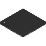
AD9511BCPZ
Active1.2 GHZCLOCK DISTRIBUTION IC, PLL CORE, DIVIDERS, DELAY ADJUST, FIVE OUTPUTS

AD9511BCPZ
Active1.2 GHZCLOCK DISTRIBUTION IC, PLL CORE, DIVIDERS, DELAY ADJUST, FIVE OUTPUTS
Description
General part information
AD9511 Series
The AD9511 provides a multi-output clock distribution function along with an on-chip PLL core. The design emphasizes low jitter and phase noise to maximize data converter performance. Other applications with demanding phase noise and jitter requirements also benefit from this part.The PLL section consists of a programmable reference divider (R); a low noise phase frequency detector (PFD); a precision charge pump (CP); and a programmable feedback divider (N). By connecting an external VCXO or VCO to the CLK2/CLK2B pins, frequencies up to 1.6 GHz may be synchronized to the input reference.There are five independent clock outputs. Three outputs are LVPECL (1.2 GHz), and two are selectable as either LVDS (800 MHz) or CMOS (250 MHz) levels.Each output has a programmable divider that may be bypassed or set to divide by any integer up to 32. The phase of one clock output relative to another clock output may be varied by means of a divider phase select function that serves as a coarse timing adjustment. One of the LVDS/CMOS outputs features a programmable delay element with full-scale ranges up to 10 ns of delay. This fine tuning delay block has 5-bit resolution, giving 32 possible delays from which to choose for each full-scale setting.The AD9511 is ideally suited for data converter clocking applications where maximum converter performance is achieved by encode signals with subpicosecond jitter.The AD9511 is available in a 48-lead LFCSP and can be operated from a single 3.3 V supply. An external VCO, which requires an extended voltage range, can be accommodated by connecting the charge pump supply (VCP) to 5.5 V. The temperature range is −40°C to +85°C.APPLICATIONSLow jitter, low phase noise clock distributionClocking high speed ADCs, DACs, DDS, DDC, DUC, MxFEsHigh performance wireless transceiversHigh performance instrumentationBroadband infrastructure
Technical Specifications
Parameters and characteristics for this part
| Specification | AD9511BCPZ |
|---|---|
| Differential Input | Yes |
| Differential Output | Yes |
| Frequency - Max | 1.2 GHz |
| Input | Clock |
| Input Ratio | 2 |
| Mounting Type | Surface Mount |
| Number of Circuits | 1 |
| Operating Temperature (Max) | 85 °C |
| Operating Temperature (Min) | -40 °C |
| Output | LVDS, CMOS, LVPECL |
| Output Ratio | 5 |
| Package / Case | 48-VFQFN Exposed Pad, CSP |
| Package Length | 7 mm |
| Package Name | 48-LFCSP-VQ |
| Package Width | 7 mm |
| Type | Divider, Fanout Buffer (Distribution) |
| Voltage - Supply (Maximum) | 3.465 V |
| Voltage - Supply (Minimum) | 3.135 V |
Pricing
Prices provided here are for design reference only. For realtime values and availability, please visit the distributors directly
Sign in to see pricing
Create a free account to access distributor pricing data.
CAD
3D models and CAD resources for this part
Documents
Technical documentation and resources