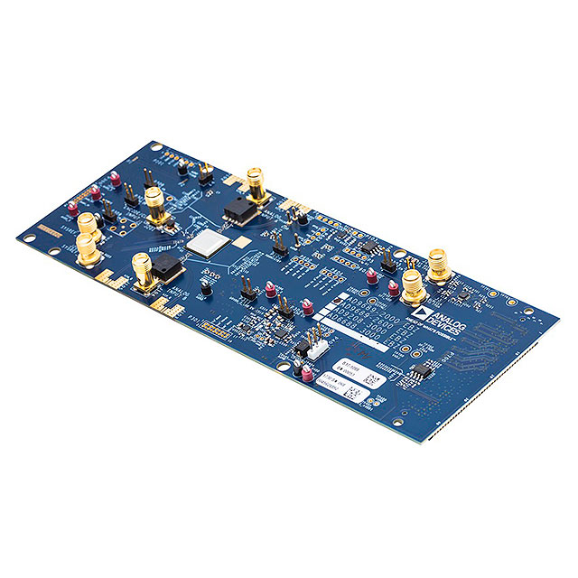
AD9689BBPZ-2000
Active2-CHANNEL DUAL ADC PIPELINED 2GSPS 14-BIT JESD204B 196-PIN TEBGA TRAY
AD9689BBPZ-2000
Active2-CHANNEL DUAL ADC PIPELINED 2GSPS 14-BIT JESD204B 196-PIN TEBGA TRAY
Description
General part information
AD9689 Series
The AD9689 is a dual, 14-bit, 2.0 GSPS/2.6 GSPS analog-to-digital converter (ADC). The device has an on-chip buffer and a sample-and-hold circuit designed for low power, small size, and ease of use. This product is designed to support communications applications capable of direct sampling wide bandwidth analog signals of up to 5 GHz. The −3 dB bandwidth of the ADC input is 9 GHz. The AD9689 is optimized for wide input bandwidth, high sampling rate, excellent linearity, and low power in a small package.The dual ADC cores feature a multistage, differential pipelined architecture with integrated output error correction logic. Each ADC features wide bandwidth inputs supporting a variety of user-selectable input ranges. An integrated voltage reference eases design considerations. The analog input and clock signals are differential inputs. The ADC data outputs are internally connected to four digital downconverters (DDCs) through a crossbar mux. Each DDC consists of multiple cascaded signal processing stages: a 48-bit frequency translator (numerically controlled oscillator (NCO)), and decimation rates. The NCO has the option to select preset bands over the general-purpose input/output (GPIO) pins, which enables the selection of up to three bands. Operation of the AD9689 between the DDC modes is selectable via SPI-programmable profiles.In addition to the DDC blocks, the AD9689 has several functions that simplify the automatic gain control (AGC) function in a communications receiver. The programmable threshold detector allows monitoring of the incoming signal power using the fast detect control bits in Register 0x0245 of the ADC. If the input signal level exceeds the programmable threshold, the fast detect indicator goes high. Because this threshold indicator has low latency, the user can quickly turn down the system gain to avoid an overrange condition at the ADC input. In addition to the fast detect outputs, the AD9689 also offers signal monitoring capability. The signal monitoring block provides additional information about the signal being digitized by the ADC.The user can configure the Subclasss 1 JESD204B-based high speed serialized output in a variety of one-lane, two-lane, four-lane, and eight-lane configurations, depending on the DDC configuration and the acceptable lane rate of the receiving logic device. Multidevice synchronization is supported through the SYSREF± and SYNCINB± input pins.The AD9689 has flexible power-down options that allow significant power savings when desired. All of these features can be programmed using a 3-wire serial port interface (SPI).The AD9689 is available in a Pb-free, 196-ball BGA, specified over the −40°C to +85°C ambient temperature range. This product is protected by a U.S. patent.Note that throughout this data sheet, multifunction pins, such as FD_A/GPIO_A0, are referred to either by the entire pin name or by a single function of the pin, for example, FD_A, when only that function is relevant.Product HighlightsWide, input −3 dB bandwidth of 9 GHz supports direct radio frequency (RF) sampling of signals up to about 5 GHz.Four integrated, wideband decimation filters and NCO blocks supporting multiband receivers.Fast NCO switching enabled through the GPIO pins.SPI controls various product features and functions to meet specific system requirements.Programmable fast overrange detection and signal monitoring.On-chip temperature diode for system thermal management.12 mm × 12 mm, 196-ball BGA.Pin, package, feature, and memory map compatible with the AD9208 14-bit, 3.0 GSPS, JESD204B dual ADC.ApplicationsDiversity multiband and multimode digital receivers3G/4G, TD-SCDMA, W-CDMA, and GSM, LTE, LTE-AElectronic test and measurement systemsPhased array radar and electronic warfareDOCSIS 3.0 CMTS upstream receive pathsHFC digital reverse path receivers
Technical Specifications
Parameters and characteristics for this part
| Specification | AD9689BBPZ-2000 |
|---|---|
| Architecture | Pipelined |
| Configuration | S/H-ADC |
| Data Interface | JESD204B |
| Input Type | Differential |
| Mounting Type | Surface Mount |
| Number of A/D Converters | 2 count |
| Number of Bits | 14 bits |
| Number of Inputs | 2 |
| Operating Temperature (Max) | 85 °C |
| Operating Temperature (Min) | -40 °C |
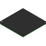
| Package / Case | 196-LFBGA Exposed Pad |
| Package Length | 12 mm |
| Package Name | 196-BGA-ED |
| Package Width | 12 mm |
| Ratio - ADC | 1 |
| Ratio - S/H | 1 |
| Reference Type | External, Internal |
| Sampling Rate (Per Second) | 2 GHz |
| Voltage - Supply, Analog (Range 1 Max) | 1 V |
| Voltage - Supply, Analog (Range 1 Min) | 0.95 V |
| Voltage - Supply, Analog (Range 2 Max) | 1.95 V |
| Voltage - Supply, Analog (Range 2 Min) | 1.85 V |
| Voltage - Supply, Analog (Range 3 Max) | 2.56 V |
| Voltage - Supply, Analog (Range 3 Min) | 2.44 V |
| Voltage - Supply, Digital (Range 1) Maximum | 1 V |
| Voltage - Supply, Digital (Range 1) Minimum | 0.95 V |
| Voltage - Supply, Digital (Range 2) Maximum | 1.95 V |
| Voltage - Supply, Digital (Range 2) Minimum | 1.85 V |
Pricing
Prices provided here are for design reference only. For realtime values and availability, please visit the distributors directly
Sign in to see pricing
Create a free account to access distributor pricing data.
CAD
3D models and CAD resources for this part
Documents
Technical documentation and resources