LTM9009CY-14#PBF
Active14-BIT, 80MSPS LOW POWER OCTAL ADCS
Deep-Dive with AI
Search across all available documentation for this part.
LTM9009CY-14#PBF
Active14-BIT, 80MSPS LOW POWER OCTAL ADCS
Technical Specifications
Parameters and characteristics for this part
| Specification | LTM9009CY-14#PBF |
|---|---|
| Architecture | Pipelined |
| Configuration | S/H-ADC |
| Data Interface | LVDS - Serial |
| Features | Simultaneous Sampling |
| Input Type | Differential |
| Mounting Type | Surface Mount |
| Number of A/D Converters | 8 |
| Number of Bits | 14 |
| Number of Inputs | 8 |
| Operating Temperature [Max] | 70 °C |
| Operating Temperature [Min] | 0 °C |
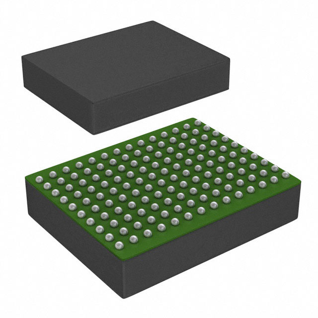
| Package / Case | 140-BFBGA |
| Ratio - S/H:ADC | 1:1 |
| Reference Type | External, Internal |
| Sampling Rate (Per Second) | 80 M |
| Supplier Device Package | 140-BGA (11.25x9) |
| Voltage - Supply, Analog [Max] | 1.9 V |
| Voltage - Supply, Analog [Min] | 1.7 V |
| Voltage - Supply, Digital [Max] | 1.9 V |
| Voltage - Supply, Digital [Min] | 1.7 V |
Pricing
Prices provided here are for design reference only. For realtime values and availability, please visit the distributors directly
| Distributor | Package | Quantity | $ | |
|---|---|---|---|---|
| Digikey | Tray | 1 | $ 173.39 | |
| 10 | $ 165.46 | |||
Description
General part information
LTM9009-14 Series
The LTM9011-14/LTM9010-14/LTM9009-14 are 8-channel, simultaneous sampling 14-bit A/D converters designed for digitizing high frequency, wide dynamic range signals. AC performance includes 73.1dB SNR and 88dB spurious free dynamic range (SFDR). Low power consumption per channel reduces heat in high channel count applications. Integrated bypass capacitance and flow-through pinout reduces overall board space requirements.DC specs include ±1LSB INL (typ), ±0.3LSB DNL (typ) and no missing codes over temperature. The transition noise is a low 1.2LSBRMS.The digital outputs are serial LVDS to minimize the number of data lines. Each channel outputs two bits at a time (2-lane mode). At lower sampling rates there is a one bit per channel option (1-lane mode).The ENC+and ENC–inputs may be driven differentially or single-ended with a sine wave, PECL, LVDS, TTL, or CMOS inputs. An internal clock duty cycle stabilizer allows high performance at full speed for a wide range of clock duty cycles.ApplicationsCommunicationsCellular Base StationsSoftware Defined RadiosPortable Medical ImagingMultichannel Data AcquisitionNondestructive Testing
Documents
Technical documentation and resources