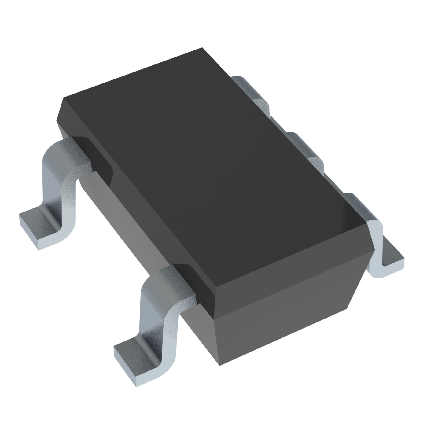
SN74LVC1G02DBVRG4
ActiveTexas Instruments
SINGLE 2-INPUT, 1.65-V TO 5.5-V NOR GATE
Deep-Dive with AI
Search across all available documentation for this part.
SN74LVC1G02DBVRG4
ActiveTexas Instruments
SINGLE 2-INPUT, 1.65-V TO 5.5-V NOR GATE
Technical Specifications
Parameters and characteristics commom to parts in this series
| Specification | SN74LVC1G02DBVRG4 | 74LVC1G02 Series |
|---|---|---|
| - | - | |
| Current - Output High, Low [custom] | 32 mA | 32 mA |
| Current - Output High, Low [custom] | 32 mA | 32 mA |
| Current - Quiescent (Max) [Max] | 10 µA | 10 µA |
| Input Logic Level - High [Max] | 2 V | 2 V |
| Input Logic Level - High [Min] | 1.7 V | 1.7 V |
| Input Logic Level - Low [Max] | 0.8 V | 0.8 V |
| Input Logic Level - Low [Min] | 0.7 V | 0.7 V |
| Logic Type | NOR Gate | NOR Gate |
| Max Propagation Delay @ V, Max CL | 4.5 ns | 4 - 5 ns |
| Mounting Type | Surface Mount | Surface Mount |
| Number of Circuits | 1 | 1 |
| Number of Inputs | 2 | 2 |
| Operating Temperature [Max] | 125 °C | 85 - 125 °C |
| Operating Temperature [Min] | -40 °C | -55 - -40 °C |
| Package / Case | SOT-753, SC-74A | SOT-553, DSBGA, 5-XFBGA, 6-XFDFN, 4-XFDFN Exposed Pad, 5-TSSOP, SOT-353, SC-70-5, 6-UFDFN, SOT-753, SC-74A |
| Supplier Device Package | SOT-23-5 | SOT-5, 5-DSBGA (1.4x0.9), 6-SON (1x1), 4-X2SON, SC-70-5, 6-SON, SOT-23-5 |
| Supplier Device Package | - | 0.8 - 1 |
| Supplier Device Package | - | 0.8 - 1.45 |
| Voltage - Supply [Max] | 5.5 V | 5.5 V |
| Voltage - Supply [Min] | 1.65 V | 1.65 V |
Pricing
Prices provided here are for design reference only. For realtime values and availability, please visit the distributors directly
74LVC1G02 Series
Single 2-input, 1.65-V to 5.5-V NOR gate
| Part | Number of Inputs | Package / Case | Operating Temperature [Max] | Operating Temperature [Min] | Current - Output High, Low [custom] | Current - Output High, Low [custom] | Logic Type | Current - Quiescent (Max) [Max] | Voltage - Supply [Max] | Voltage - Supply [Min] | Input Logic Level - High [Min] | Input Logic Level - High [Max] | Input Logic Level - Low [Max] | Input Logic Level - Low [Min] | Max Propagation Delay @ V, Max CL | Mounting Type | Number of Circuits | Supplier Device Package | Supplier Device Package [y] | Supplier Device Package [x] |
|---|---|---|---|---|---|---|---|---|---|---|---|---|---|---|---|---|---|---|---|---|
Texas Instruments SN74LVC1G02DRLRThis single 2-input positive-NOR gate is designed for 1.65-V to 5.5-V VCCoperation.
The SN74LVC1G02 performs the Boolean functionY =A + Bor Y =A•Bin positive logic.
The CMOS device has high output drive while maintaining low static power dissipation over a broad VCCoperating range.
The SN74LVC1G02 device is available in a variety of packages, including the ultra-small DPW package with a body size of 0.8 × 0.8 mm.
This single 2-input positive-NOR gate is designed for 1.65-V to 5.5-V VCCoperation.
The SN74LVC1G02 performs the Boolean functionY =A + Bor Y =A•Bin positive logic.
The CMOS device has high output drive while maintaining low static power dissipation over a broad VCCoperating range.
The SN74LVC1G02 device is available in a variety of packages, including the ultra-small DPW package with a body size of 0.8 × 0.8 mm. | 2 | SOT-553 | 125 °C | -40 °C | 32 mA | 32 mA | NOR Gate | 10 µA | 5.5 V | 1.65 V | 1.7 V | 2 V | 0.8 V | 0.7 V | 4.5 ns | Surface Mount | 1 | SOT-5 | ||
2 | 5-XFBGA, DSBGA | 85 °C | -40 °C | 32 mA | 32 mA | NOR Gate | 10 µA | 5.5 V | 1.65 V | 1.7 V | 2 V | 0.8 V | 0.7 V | 4 ns | Surface Mount | 1 | 5-DSBGA (1.4x0.9) | |||
2 | 5-XFBGA, DSBGA | 85 °C | -40 °C | 32 mA | 32 mA | NOR Gate | 10 µA | 5.5 V | 1.65 V | 1.7 V | 2 V | 0.8 V | 0.7 V | 4 ns | Surface Mount | 1 | 5-DSBGA (1.4x0.9) | |||
Texas Instruments SN74LVC1G02DSFRThis single 2-input positive-NOR gate is designed for 1.65-V to 5.5-V VCCoperation.
The SN74LVC1G02 performs the Boolean functionY =A + Bor Y =A•Bin positive logic.
The CMOS device has high output drive while maintaining low static power dissipation over a broad VCCoperating range.
The SN74LVC1G02 device is available in a variety of packages, including the ultra-small DPW package with a body size of 0.8 × 0.8 mm.
This single 2-input positive-NOR gate is designed for 1.65-V to 5.5-V VCCoperation.
The SN74LVC1G02 performs the Boolean functionY =A + Bor Y =A•Bin positive logic.
The CMOS device has high output drive while maintaining low static power dissipation over a broad VCCoperating range.
The SN74LVC1G02 device is available in a variety of packages, including the ultra-small DPW package with a body size of 0.8 × 0.8 mm. | 2 | 6-XFDFN | 125 °C | -40 °C | 32 mA | 32 mA | NOR Gate | 10 µA | 5.5 V | 1.65 V | 1.7 V | 2 V | 0.8 V | 0.7 V | 4.5 ns | Surface Mount | 1 | 6-SON (1x1) | ||
Texas Instruments SN74LVC1G02DPWRThis single 2-input positive-NOR gate is designed for 1.65-V to 5.5-V VCCoperation.
The SN74LVC1G02 performs the Boolean functionY =A + Bor Y =A•Bin positive logic.
The CMOS device has high output drive while maintaining low static power dissipation over a broad VCCoperating range.
The SN74LVC1G02 device is available in a variety of packages, including the ultra-small DPW package with a body size of 0.8 × 0.8 mm.
This single 2-input positive-NOR gate is designed for 1.65-V to 5.5-V VCCoperation.
The SN74LVC1G02 performs the Boolean functionY =A + Bor Y =A•Bin positive logic.
The CMOS device has high output drive while maintaining low static power dissipation over a broad VCCoperating range.
The SN74LVC1G02 device is available in a variety of packages, including the ultra-small DPW package with a body size of 0.8 × 0.8 mm. | 2 | 4-XFDFN Exposed Pad | 125 °C | -40 °C | 32 mA | 32 mA | NOR Gate | 10 µA | 5.5 V | 1.65 V | 1.7 V | 2 V | 0.8 V | 0.7 V | 4.5 ns | Surface Mount | 1 | 4-X2SON | 0.8 | 0.8 |
Texas Instruments SN74LVC1G02DCKRG4This single 2-input positive-NOR gate is designed for 1.65-V to 5.5-V VCCoperation.
The SN74LVC1G02 performs the Boolean functionY =A + Bor Y =A•Bin positive logic.
The CMOS device has high output drive while maintaining low static power dissipation over a broad VCCoperating range.
The SN74LVC1G02 device is available in a variety of packages, including the ultra-small DPW package with a body size of 0.8 × 0.8 mm.
This single 2-input positive-NOR gate is designed for 1.65-V to 5.5-V VCCoperation.
The SN74LVC1G02 performs the Boolean functionY =A + Bor Y =A•Bin positive logic.
The CMOS device has high output drive while maintaining low static power dissipation over a broad VCCoperating range.
The SN74LVC1G02 device is available in a variety of packages, including the ultra-small DPW package with a body size of 0.8 × 0.8 mm. | 2 | 5-TSSOP, SC-70-5, SOT-353 | 125 °C | -40 °C | 32 mA | 32 mA | NOR Gate | 10 µA | 5.5 V | 1.65 V | 1.7 V | 2 V | 0.8 V | 0.7 V | 4.5 ns | Surface Mount | 1 | SC-70-5 | ||
Texas Instruments SN74LVC1G02DRYRThis single 2-input positive-NOR gate is designed for 1.65-V to 5.5-V VCCoperation.
The SN74LVC1G02 performs the Boolean functionY =A + Bor Y =A•Bin positive logic.
The CMOS device has high output drive while maintaining low static power dissipation over a broad VCCoperating range.
The SN74LVC1G02 device is available in a variety of packages, including the ultra-small DPW package with a body size of 0.8 × 0.8 mm.
This single 2-input positive-NOR gate is designed for 1.65-V to 5.5-V VCCoperation.
The SN74LVC1G02 performs the Boolean functionY =A + Bor Y =A•Bin positive logic.
The CMOS device has high output drive while maintaining low static power dissipation over a broad VCCoperating range.
The SN74LVC1G02 device is available in a variety of packages, including the ultra-small DPW package with a body size of 0.8 × 0.8 mm. | 2 | 6-UFDFN | 125 °C | -40 °C | 32 mA | 32 mA | NOR Gate | 10 µA | 5.5 V | 1.65 V | 1.7 V | 2 V | 0.8 V | 0.7 V | 4.5 ns | Surface Mount | 1 | 6-SON | 1 | 1.45 |
Texas Instruments SN74LVC1G02MDCKREPThis single 2-input positive-NOR gate is designed for 1.65-V to 5.5-V VCCoperation.
The SN74LVC1G02 performs the Boolean function Y =A + Bor Y =A×Bin positive logic.
NanoStar™ and NanoFree™ package technology is a major breakthrough in IC packaging concepts, using the die as the package.
This device is fully specified for partial-power-down applications using Ioff. The Ioffcircuitry disables the outputs, preventing damaging current backflow through the device when it is powered down.
This single 2-input positive-NOR gate is designed for 1.65-V to 5.5-V VCCoperation.
The SN74LVC1G02 performs the Boolean function Y =A + Bor Y =A×Bin positive logic.
NanoStar™ and NanoFree™ package technology is a major breakthrough in IC packaging concepts, using the die as the package.
This device is fully specified for partial-power-down applications using Ioff. The Ioffcircuitry disables the outputs, preventing damaging current backflow through the device when it is powered down. | 2 | 5-TSSOP, SC-70-5, SOT-353 | 125 °C | -55 °C | 32 mA | 32 mA | NOR Gate | 10 µA | 5.5 V | 1.65 V | 1.7 V | 2 V | 0.8 V | 0.7 V | 5 ns | Surface Mount | 1 | SC-70-5 | ||
2 | 5-XFBGA, DSBGA | 85 °C | -40 °C | 32 mA | 32 mA | NOR Gate | 10 µA | 5.5 V | 1.65 V | 1.7 V | 2 V | 0.8 V | 0.7 V | 4 ns | Surface Mount | 1 | 5-DSBGA (1.4x0.9) | |||
Texas Instruments SN74LVC1G02DBVTG4This single 2-input positive-NOR gate is designed for 1.65-V to 5.5-V VCCoperation.
The SN74LVC1G02 performs the Boolean functionY =A + Bor Y =A•Bin positive logic.
The CMOS device has high output drive while maintaining low static power dissipation over a broad VCCoperating range.
The SN74LVC1G02 device is available in a variety of packages, including the ultra-small DPW package with a body size of 0.8 × 0.8 mm.
This single 2-input positive-NOR gate is designed for 1.65-V to 5.5-V VCCoperation.
The SN74LVC1G02 performs the Boolean functionY =A + Bor Y =A•Bin positive logic.
The CMOS device has high output drive while maintaining low static power dissipation over a broad VCCoperating range.
The SN74LVC1G02 device is available in a variety of packages, including the ultra-small DPW package with a body size of 0.8 × 0.8 mm. | 2 | SC-74A, SOT-753 | 125 °C | -40 °C | 32 mA | 32 mA | NOR Gate | 10 µA | 5.5 V | 1.65 V | 1.7 V | 2 V | 0.8 V | 0.7 V | 4.5 ns | Surface Mount | 1 | SOT-23-5 | ||
2 | 5-TSSOP, SC-70-5, SOT-353 | 125 °C | -40 °C | 32 mA | 32 mA | NOR Gate | 10 µA | 5.5 V | 1.65 V | 1.7 V | 2 V | 0.8 V | 0.7 V | 4.5 ns | Surface Mount | 1 | SC-70-5 | |||
Texas Instruments SN74LVC1G02DCKRThis single 2-input positive-NOR gate is designed for 1.65-V to 5.5-V VCCoperation.
The SN74LVC1G02 performs the Boolean functionY =A + Bor Y =A•Bin positive logic.
The CMOS device has high output drive while maintaining low static power dissipation over a broad VCCoperating range.
The SN74LVC1G02 device is available in a variety of packages, including the ultra-small DPW package with a body size of 0.8 × 0.8 mm.
This single 2-input positive-NOR gate is designed for 1.65-V to 5.5-V VCCoperation.
The SN74LVC1G02 performs the Boolean functionY =A + Bor Y =A•Bin positive logic.
The CMOS device has high output drive while maintaining low static power dissipation over a broad VCCoperating range.
The SN74LVC1G02 device is available in a variety of packages, including the ultra-small DPW package with a body size of 0.8 × 0.8 mm. | 2 | 5-TSSOP, SC-70-5, SOT-353 | 125 °C | -40 °C | 32 mA | 32 mA | NOR Gate | 10 µA | 5.5 V | 1.65 V | 1.7 V | 2 V | 0.8 V | 0.7 V | 4.5 ns | Surface Mount | 1 | SC-70-5 | ||
Texas Instruments SN74LVC1G02DCKTThis single 2-input positive-NOR gate is designed for 1.65-V to 5.5-V VCCoperation.
The SN74LVC1G02 performs the Boolean functionY =A + Bor Y =A•Bin positive logic.
The CMOS device has high output drive while maintaining low static power dissipation over a broad VCCoperating range.
The SN74LVC1G02 device is available in a variety of packages, including the ultra-small DPW package with a body size of 0.8 × 0.8 mm.
This single 2-input positive-NOR gate is designed for 1.65-V to 5.5-V VCCoperation.
The SN74LVC1G02 performs the Boolean functionY =A + Bor Y =A•Bin positive logic.
The CMOS device has high output drive while maintaining low static power dissipation over a broad VCCoperating range.
The SN74LVC1G02 device is available in a variety of packages, including the ultra-small DPW package with a body size of 0.8 × 0.8 mm. | 2 | 5-TSSOP, SC-70-5, SOT-353 | 125 °C | -40 °C | 32 mA | 32 mA | NOR Gate | 10 µA | 5.5 V | 1.65 V | 1.7 V | 2 V | 0.8 V | 0.7 V | 4.5 ns | Surface Mount | 1 | SC-70-5 | ||
Texas Instruments SN74LVC1G02YZPRThis single 2-input positive-NOR gate is designed for 1.65-V to 5.5-V VCCoperation.
The SN74LVC1G02 performs the Boolean functionY =A + Bor Y =A•Bin positive logic.
The CMOS device has high output drive while maintaining low static power dissipation over a broad VCCoperating range.
The SN74LVC1G02 device is available in a variety of packages, including the ultra-small DPW package with a body size of 0.8 × 0.8 mm.
This single 2-input positive-NOR gate is designed for 1.65-V to 5.5-V VCCoperation.
The SN74LVC1G02 performs the Boolean functionY =A + Bor Y =A•Bin positive logic.
The CMOS device has high output drive while maintaining low static power dissipation over a broad VCCoperating range.
The SN74LVC1G02 device is available in a variety of packages, including the ultra-small DPW package with a body size of 0.8 × 0.8 mm. | 2 | 5-XFBGA, DSBGA | 85 °C | -40 °C | 32 mA | 32 mA | NOR Gate | 10 µA | 5.5 V | 1.65 V | 1.7 V | 2 V | 0.8 V | 0.7 V | 4 ns | Surface Mount | 1 | 5-DSBGA (1.4x0.9) | ||
Texas Instruments SN74LVC1G02DBVRG4This single 2-input positive-NOR gate is designed for 1.65-V to 5.5-V VCCoperation.
The SN74LVC1G02 performs the Boolean functionY =A + Bor Y =A•Bin positive logic.
The CMOS device has high output drive while maintaining low static power dissipation over a broad VCCoperating range.
The SN74LVC1G02 device is available in a variety of packages, including the ultra-small DPW package with a body size of 0.8 × 0.8 mm.
This single 2-input positive-NOR gate is designed for 1.65-V to 5.5-V VCCoperation.
The SN74LVC1G02 performs the Boolean functionY =A + Bor Y =A•Bin positive logic.
The CMOS device has high output drive while maintaining low static power dissipation over a broad VCCoperating range.
The SN74LVC1G02 device is available in a variety of packages, including the ultra-small DPW package with a body size of 0.8 × 0.8 mm. | 2 | SC-74A, SOT-753 | 125 °C | -40 °C | 32 mA | 32 mA | NOR Gate | 10 µA | 5.5 V | 1.65 V | 1.7 V | 2 V | 0.8 V | 0.7 V | 4.5 ns | Surface Mount | 1 | SOT-23-5 | ||
Texas Instruments SN74LVC1G02DRY2This single 2-input positive-NOR gate is designed for 1.65-V to 5.5-V VCCoperation.
The SN74LVC1G02 performs the Boolean functionY =A + Bor Y =A•Bin positive logic.
The CMOS device has high output drive while maintaining low static power dissipation over a broad VCCoperating range.
The SN74LVC1G02 device is available in a variety of packages, including the ultra-small DPW package with a body size of 0.8 × 0.8 mm.
This single 2-input positive-NOR gate is designed for 1.65-V to 5.5-V VCCoperation.
The SN74LVC1G02 performs the Boolean functionY =A + Bor Y =A•Bin positive logic.
The CMOS device has high output drive while maintaining low static power dissipation over a broad VCCoperating range.
The SN74LVC1G02 device is available in a variety of packages, including the ultra-small DPW package with a body size of 0.8 × 0.8 mm. | 2 | 6-UFDFN | 125 °C | -40 °C | 32 mA | 32 mA | NOR Gate | 10 µA | 5.5 V | 1.65 V | 1.7 V | 2 V | 0.8 V | 0.7 V | 4.5 ns | Surface Mount | 1 | 6-SON | 1 | 1.45 |
Texas Instruments SN74LVC1G02DBVRThis single 2-input positive-NOR gate is designed for 1.65-V to 5.5-V VCCoperation.
The SN74LVC1G02 performs the Boolean functionY =A + Bor Y =A•Bin positive logic.
The CMOS device has high output drive while maintaining low static power dissipation over a broad VCCoperating range.
The SN74LVC1G02 device is available in a variety of packages, including the ultra-small DPW package with a body size of 0.8 × 0.8 mm.
This single 2-input positive-NOR gate is designed for 1.65-V to 5.5-V VCCoperation.
The SN74LVC1G02 performs the Boolean functionY =A + Bor Y =A•Bin positive logic.
The CMOS device has high output drive while maintaining low static power dissipation over a broad VCCoperating range.
The SN74LVC1G02 device is available in a variety of packages, including the ultra-small DPW package with a body size of 0.8 × 0.8 mm. | 2 | SC-74A, SOT-753 | 125 °C | -40 °C | 32 mA | 32 mA | NOR Gate | 10 µA | 5.5 V | 1.65 V | 1.7 V | 2 V | 0.8 V | 0.7 V | 4.5 ns | Surface Mount | 1 | SOT-23-5 | ||
2 | SC-74A, SOT-753 | 125 °C | -40 °C | 32 mA | 32 mA | NOR Gate | 10 µA | 5.5 V | 1.65 V | 1.7 V | 2 V | 0.8 V | 0.7 V | 4.5 ns | Surface Mount | 1 | SOT-23-5 | |||
Texas Instruments SN74LVC1G02DSF2This single 2-input positive-NOR gate is designed for 1.65-V to 5.5-V VCCoperation.
The SN74LVC1G02 performs the Boolean functionY =A + Bor Y =A•Bin positive logic.
The CMOS device has high output drive while maintaining low static power dissipation over a broad VCCoperating range.
The SN74LVC1G02 device is available in a variety of packages, including the ultra-small DPW package with a body size of 0.8 × 0.8 mm.
This single 2-input positive-NOR gate is designed for 1.65-V to 5.5-V VCCoperation.
The SN74LVC1G02 performs the Boolean functionY =A + Bor Y =A•Bin positive logic.
The CMOS device has high output drive while maintaining low static power dissipation over a broad VCCoperating range.
The SN74LVC1G02 device is available in a variety of packages, including the ultra-small DPW package with a body size of 0.8 × 0.8 mm. | 2 | 6-XFDFN | 125 °C | -40 °C | 32 mA | 32 mA | NOR Gate | 10 µA | 5.5 V | 1.65 V | 1.7 V | 2 V | 0.8 V | 0.7 V | 4.5 ns | Surface Mount | 1 | 6-SON (1x1) |
Description
General part information
74LVC1G02 Series
This single 2-input positive-NOR gate is designed for 1.65-V to 5.5-V VCCoperation.
The SN74LVC1G02 performs the Boolean functionY =A + Bor Y =A•Bin positive logic.
The CMOS device has high output drive while maintaining low static power dissipation over a broad VCCoperating range.
Documents
Technical documentation and resources