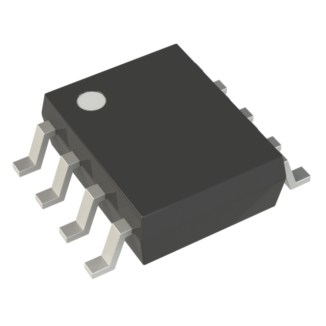
Technical Specifications
Parameters and characteristics for this part
| Specification | TDE1707BFPT |
|---|---|
| Current - Output (Max) [Max] | 500 mA |
| Fault Protection | Over Temperature, Current Limiting (Fixed) |
| Features | 5V Regulated Output |
| Input Type | Non-Inverting |
| Interface | On/Off |
| Mounting Type | Surface Mount |
| Number of Outputs | 2 |
| Operating Temperature [Max] | 85 C |
| Operating Temperature [Min] | -25 °C |
| Output Configuration | High Side or Low Side |
| Output Type | Bipolar |
| Package / Case | 8-SOIC |
| Package / Case [x] | 0.154 in |
| Package / Case [y] | 3.9 mm |
| Ratio - Input:Output [custom] | 1:2 |
| Supplier Device Package | 8-SOIC |
| Switch Type | General Purpose |
| Voltage - Load [Max] | 48 V |
| Voltage - Load [Min] | 6 V |
| Voltage - Supply (Vcc/Vdd) | False |
Pricing
Prices provided here are for design reference only. For realtime values and availability, please visit the distributors directly
| Distributor | Package | Quantity | $ | |
|---|---|---|---|---|
| Digikey | Cut Tape (CT) | 1 | $ 4.68 | |
| 10 | $ 4.21 | |||
| 25 | $ 3.98 | |||
| 100 | $ 3.45 | |||
| 250 | $ 3.27 | |||
| 500 | $ 2.93 | |||
| 1000 | $ 2.47 | |||
| Digi-Reel® | 1 | $ 4.68 | ||
| 10 | $ 4.21 | |||
| 25 | $ 3.98 | |||
| 100 | $ 3.45 | |||
| 250 | $ 3.27 | |||
| 500 | $ 2.93 | |||
| 1000 | $ 2.47 | |||
| Tape & Reel (TR) | 2500 | $ 2.35 | ||
Description
General part information
TDE1707 Series
The TDE1707BFP and TDE1707CFP are 0.5 A integrated power switches with up to 48 V power supply capability. Two output configurations are possible. The former is the load to GND (high-side mode) and the latter is the load to VS(low-side mode). This device is dedicated to proximity detectors; its internal +5 V supply can be used to supply external circuits (please refer to AN495 and AN1213 on www.st.com). A signal is internally generated to block the IN signal, and prevent the output switch, as long as an abnormal condition is detected. The power-on transition, as well as the chip overtemperature and the output overcurrent, generate this signal. A minimum delay of 25 μs (typ. value) is added to the trailing edge of this signal to ensure that a stable normal situation is present when the signal disappears. The delay (the disappearance of block signal) can be further increased by connecting a capacitor between pin 3 and ground. It can drive resistive or inductive loads.
Documents
Technical documentation and resources


