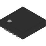
ADL8122ACPZN
Active10 KHZ TO 10 GHZ, WIDEBAND, LOW NOISE AMPLIFIER
ADL8122ACPZN
Active10 KHZ TO 10 GHZ, WIDEBAND, LOW NOISE AMPLIFIER
Description
General part information
ADL8122 Series
The ADL8122 is a wideband low noise amplifier (LNA) that operates from 10 kHz to 10 GHz. Typical gain and noise figure are 17 dB and 2 dB, respectively, from 2 GHz to 6 GHz. Output power for 1 dB compression (OP1dB), output third-order intercept (OIP3), and output second-order intercept (OIP2) are 20 dBm, 33.5 dBm, and 37 dBm, respectively, from 2 GHz to 6 GHz. The nominal quiescent current (IDQ), which can be adjusted, is 95 mA from a 5 V supply voltage (VDD). The internally matched, DC-coupled RF input and output pins require external AC coupling capacitors along with a bias inductor on RFOUT. In addition, the RF input is biased through an external inductor connected between the VBIAS pin and the RFIN pin.The ADL8122 is fabricated on a pseudomorphic, high electron mobility transistor (pHEMT) process. The device is housed in a RoHS-compliant, 2 mm × 2 mm, 8-lead LFCSP and is specified for operation from −55°C to +125°C.APPLICATIONSTelecommunicationsInstrumentationRadarElectronic warfare
Technical Specifications
Parameters and characteristics for this part
| Specification | ADL8122ACPZN |
|---|---|
| Current - Supply | 90 mA |
| Frequency Range 1 (Max) | 10 GHz |
| Frequency Range 1 (Min) | 10 kHz |
| Gain | 17.5 dB |
| Mounting Type | Surface Mount |
| Noise Figure | 2.5 dB |
| P1dB | 20.5 dBm |
| Package / Case | 8-VFDFN Exposed Pad, CSP |
| Package Length | 2 mm |
| Package Name | 8-LFCSP |
| Package Width | 2 mm |
| RF Type | Radar |
| Test Frequency (Maximum) | 2 GHz |
| Test Frequency (Minimum) | 10 kHz |
| Voltage - Supply (Maximum) | 6 V |
| Voltage - Supply (Minimum) | 3 V |
Pricing
Prices provided here are for design reference only. For realtime values and availability, please visit the distributors directly
Sign in to see pricing
Create a free account to access distributor pricing data.
CAD
3D models and CAD resources for this part
Documents
Technical documentation and resources