SN74LVC1G08MDBVREP
ActiveENHANCED PRODUCT, 1-CH, 2-INPUT 1.65-V TO 5.5-V 32-MA DRIVE STRENGTH AND GATE
Deep-Dive with AI
Search across all available documentation for this part.
SN74LVC1G08MDBVREP
ActiveENHANCED PRODUCT, 1-CH, 2-INPUT 1.65-V TO 5.5-V 32-MA DRIVE STRENGTH AND GATE
Deep-Dive with AI
Technical Specifications
Parameters and characteristics commom to parts in this series
| Specification | SN74LVC1G08MDBVREP | 74LVC1G08 Series |
|---|---|---|
| - | - | |
| Current - Output High, Low [custom] | 32 mA | 32 mA |
| Current - Output High, Low [custom] | 32 mA | 32 mA |
| Current - Quiescent (Max) [Max] | 10 µA | 10 µA |
| Grade | - | Automotive |
| Input Logic Level - High | - | 1.7 V |
| Input Logic Level - High | - | 2 V |
| Input Logic Level - Low | - | 0.8 V |
| Input Logic Level - Low | - | 0.7 V |
| Logic Type | AND Gate | AND Gate |
| Max Propagation Delay @ V, Max CL | 5 ns | 4 - 6 ns |
| Mounting Type | Surface Mount | Surface Mount |
| Number of Circuits | 1 | 1 |
| Number of Inputs | 2 | 2 |
| Operating Temperature [Max] | 125 °C | 85 - 125 °C |
| Operating Temperature [Min] | -55 °C | -55 - -40 °C |
| Package / Case | SOT-753, SC-74A | 6-XFDFN, SOT-753, SC-74A, 6-UFDFN, 5-TSSOP, SOT-353, SC-70-5, DSBGA, 5-XFBGA, SOT-553, 4-XFDFN Exposed Pad |
| Qualification | - | AEC-Q100 |
| Supplier Device Package | SOT-23-5 | 6-SON (1x1), SOT-23-5, 6-SON, SC-70-5, 5-DSBGA (1.4x0.9), SOT-5, 4-X2SON |
| Supplier Device Package | - | 0.8 - 1 |
| Supplier Device Package | - | 0.8 - 1.45 |
| Voltage - Supply [Max] | 5.5 V | 5.5 V |
| Voltage - Supply [Min] | 1.65 V | 1.65 V |
Pricing
Prices provided here are for design reference only. For realtime values and availability, please visit the distributors directly
74LVC1G08 Series
1-ch, 2-input 1.65-V to 5.5-V 32 mA drive strength AND gate
| Part | Max Propagation Delay @ V, Max CL | Number of Circuits | Mounting Type | Number of Inputs | Current - Output High, Low [custom] | Current - Output High, Low [custom] | Operating Temperature [Min] | Operating Temperature [Max] | Supplier Device Package | Voltage - Supply [Max] | Voltage - Supply [Min] | Logic Type | Current - Quiescent (Max) [Max] | Package / Case | Supplier Device Package [y] | Supplier Device Package [x] | Input Logic Level - High [Min] | Input Logic Level - High [Max] | Input Logic Level - Low [Max] | Input Logic Level - Low [Min] | Qualification | Grade |
|---|---|---|---|---|---|---|---|---|---|---|---|---|---|---|---|---|---|---|---|---|---|---|
Texas Instruments SN74LVC1G08DSFRThis single 2-input positive-AND gate is designed for 1.65-V to 5.5-V VCCoperation.
The SN74LVC1G08 device performs the Boolean function or in positive logic.
The CMOS device has high output drive while maintaining low static power dissipation over a broad VCCoperating range.
The SN74LVC1G08 is available in a variety of packages, including the ultra-small DPW package with a body size of 0.8 mm × 0.8 mm.
This single 2-input positive-AND gate is designed for 1.65-V to 5.5-V VCCoperation.
The SN74LVC1G08 device performs the Boolean function or in positive logic.
The CMOS device has high output drive while maintaining low static power dissipation over a broad VCCoperating range.
The SN74LVC1G08 is available in a variety of packages, including the ultra-small DPW package with a body size of 0.8 mm × 0.8 mm. | 4 ns | 1 | Surface Mount | 2 | 32 mA | 32 mA | -40 °C | 125 °C | 6-SON (1x1) | 5.5 V | 1.65 V | AND Gate | 10 µA | 6-XFDFN | ||||||||
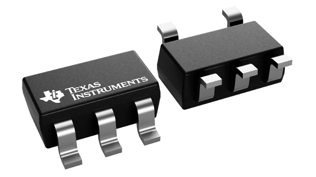
Texas Instruments SN74LVC1G08MDBVREPThe SN74LVC1G08 performs the Boolean function Y = A • B or Y =A\ + B\in positive logic.
This device is fully specified for partial-power-down applications using Ioff. The Ioffcircuitry disables the outputs, preventing damaging current backflow through the device when it is powered down.
The SN74LVC1G08 performs the Boolean function Y = A • B or Y =A\ + B\in positive logic.
This device is fully specified for partial-power-down applications using Ioff. The Ioffcircuitry disables the outputs, preventing damaging current backflow through the device when it is powered down. | 5 ns | 1 | Surface Mount | 2 | 32 mA | 32 mA | -55 °C | 125 °C | SOT-23-5 | 5.5 V | 1.65 V | AND Gate | 10 µA | SC-74A, SOT-753 | ||||||||
4 ns | 1 | Surface Mount | 2 | 32 mA | 32 mA | -40 °C | 125 °C | SOT-23-5 | 5.5 V | 1.65 V | AND Gate | 10 µA | SC-74A, SOT-753 | |||||||||
Texas Instruments SN74LVC1G08DRYRThis single 2-input positive-AND gate is designed for 1.65-V to 5.5-V VCCoperation.
The SN74LVC1G08 device performs the Boolean function or in positive logic.
The CMOS device has high output drive while maintaining low static power dissipation over a broad VCCoperating range.
The SN74LVC1G08 is available in a variety of packages, including the ultra-small DPW package with a body size of 0.8 mm × 0.8 mm.
This single 2-input positive-AND gate is designed for 1.65-V to 5.5-V VCCoperation.
The SN74LVC1G08 device performs the Boolean function or in positive logic.
The CMOS device has high output drive while maintaining low static power dissipation over a broad VCCoperating range.
The SN74LVC1G08 is available in a variety of packages, including the ultra-small DPW package with a body size of 0.8 mm × 0.8 mm. | 4 ns | 1 | Surface Mount | 2 | 32 mA | 32 mA | -40 °C | 125 °C | 6-SON | 5.5 V | 1.65 V | AND Gate | 10 µA | 6-UFDFN | 1 | 1.45 | ||||||
Texas Instruments SN74LVC1G08DCKTThis single 2-input positive-AND gate is designed for 1.65-V to 5.5-V VCCoperation.
The SN74LVC1G08 device performs the Boolean function or in positive logic.
The CMOS device has high output drive while maintaining low static power dissipation over a broad VCCoperating range.
The SN74LVC1G08 is available in a variety of packages, including the ultra-small DPW package with a body size of 0.8 mm × 0.8 mm.
This single 2-input positive-AND gate is designed for 1.65-V to 5.5-V VCCoperation.
The SN74LVC1G08 device performs the Boolean function or in positive logic.
The CMOS device has high output drive while maintaining low static power dissipation over a broad VCCoperating range.
The SN74LVC1G08 is available in a variety of packages, including the ultra-small DPW package with a body size of 0.8 mm × 0.8 mm. | 4 ns | 1 | Surface Mount | 2 | 32 mA | 32 mA | -40 °C | 125 °C | SC-70-5 | 5.5 V | 1.65 V | AND Gate | 10 µA | 5-TSSOP, SC-70-5, SOT-353 | ||||||||
Texas Instruments SN74LVC1G08DRY2This single 2-input positive-AND gate is designed for 1.65-V to 5.5-V VCCoperation.
The SN74LVC1G08 device performs the Boolean function or in positive logic.
The CMOS device has high output drive while maintaining low static power dissipation over a broad VCCoperating range.
The SN74LVC1G08 is available in a variety of packages, including the ultra-small DPW package with a body size of 0.8 mm × 0.8 mm.
This single 2-input positive-AND gate is designed for 1.65-V to 5.5-V VCCoperation.
The SN74LVC1G08 device performs the Boolean function or in positive logic.
The CMOS device has high output drive while maintaining low static power dissipation over a broad VCCoperating range.
The SN74LVC1G08 is available in a variety of packages, including the ultra-small DPW package with a body size of 0.8 mm × 0.8 mm. | 4 ns | 1 | Surface Mount | 2 | 32 mA | 32 mA | -40 °C | 125 °C | 6-SON | 5.5 V | 1.65 V | AND Gate | 10 µA | 6-UFDFN | 1 | 1.45 | ||||||
Texas Instruments SN74LVC1G08IDCKREPThe SN74LVC1G08 performs the Boolean function Y = A • B or Y =A\ + B\in positive logic.
This device is fully specified for partial-power-down applications using Ioff. The Ioffcircuitry disables the outputs, preventing damaging current backflow through the device when it is powered down.
The SN74LVC1G08 performs the Boolean function Y = A • B or Y =A\ + B\in positive logic.
This device is fully specified for partial-power-down applications using Ioff. The Ioffcircuitry disables the outputs, preventing damaging current backflow through the device when it is powered down. | 4 ns | 1 | Surface Mount | 2 | 32 mA | 32 mA | -40 °C | 85 °C | SC-70-5 | 5.5 V | 1.65 V | AND Gate | 10 µA | 5-TSSOP, SC-70-5, SOT-353 | ||||||||
Texas Instruments SN74LVC1G08DCK3This single 2-input positive-AND gate is designed for 1.65-V to 5.5-V VCCoperation.
The SN74LVC1G08 device performs the Boolean function or in positive logic.
The CMOS device has high output drive while maintaining low static power dissipation over a broad VCCoperating range.
The SN74LVC1G08 is available in a variety of packages, including the ultra-small DPW package with a body size of 0.8 mm × 0.8 mm.
This single 2-input positive-AND gate is designed for 1.65-V to 5.5-V VCCoperation.
The SN74LVC1G08 device performs the Boolean function or in positive logic.
The CMOS device has high output drive while maintaining low static power dissipation over a broad VCCoperating range.
The SN74LVC1G08 is available in a variety of packages, including the ultra-small DPW package with a body size of 0.8 mm × 0.8 mm. | 5 ns | 1 | Surface Mount | 2 | 32 mA | 32 mA | -40 °C | 125 °C | SC-70-5 | 5.5 V | 1.65 V | AND Gate | 10 µA | 5-TSSOP, SC-70-5, SOT-353 | 1.7 V | 2 V | 0.8 V | 0.7 V | ||||
Texas Instruments SN74LVC1G08IDCKRQ1This single 2-input positive-AND gate is designed for 1.65-V to 5.5-V VCCoperation.
The SN74LVC1G08-Q1 device performs the Boolean function or in positive logic.
This device is fully specified for partial-power-down applications using I off. The I off circuitry disables the outputs, preventing damaging current backflow through the device when it is powered down.
The CMOS device has high output drive while maintaining low static power dissipation over a broad VCCoperating range.
The SN74LVC1G08 is available in a variety of packages, including the small DRY package with a body size of 1.45 mm × 1.00 mm.
This single 2-input positive-AND gate is designed for 1.65-V to 5.5-V VCCoperation.
The SN74LVC1G08-Q1 device performs the Boolean function or in positive logic.
This device is fully specified for partial-power-down applications using I off. The I off circuitry disables the outputs, preventing damaging current backflow through the device when it is powered down.
The CMOS device has high output drive while maintaining low static power dissipation over a broad VCCoperating range.
The SN74LVC1G08 is available in a variety of packages, including the small DRY package with a body size of 1.45 mm × 1.00 mm. | 4 ns | 1 | Surface Mount | 2 | 32 mA | 32 mA | -40 °C | 85 °C | SC-70-5 | 5.5 V | 1.65 V | AND Gate | 10 µA | 5-TSSOP, SC-70-5, SOT-353 | AEC-Q100 | Automotive | ||||||
Texas Instruments SN74LVC1G08DSF2This single 2-input positive-AND gate is designed for 1.65-V to 5.5-V VCCoperation.
The SN74LVC1G08 device performs the Boolean function or in positive logic.
The CMOS device has high output drive while maintaining low static power dissipation over a broad VCCoperating range.
The SN74LVC1G08 is available in a variety of packages, including the ultra-small DPW package with a body size of 0.8 mm × 0.8 mm.
This single 2-input positive-AND gate is designed for 1.65-V to 5.5-V VCCoperation.
The SN74LVC1G08 device performs the Boolean function or in positive logic.
The CMOS device has high output drive while maintaining low static power dissipation over a broad VCCoperating range.
The SN74LVC1G08 is available in a variety of packages, including the ultra-small DPW package with a body size of 0.8 mm × 0.8 mm. | 4 ns | 1 | Surface Mount | 2 | 32 mA | 32 mA | -40 °C | 125 °C | 6-SON (1x1) | 5.5 V | 1.65 V | AND Gate | 10 µA | 6-XFDFN | ||||||||
4 ns | 1 | Surface Mount | 2 | 32 mA | 32 mA | -40 °C | 85 °C | 5-DSBGA (1.4x0.9) | 5.5 V | 1.65 V | AND Gate | 10 µA | 5-XFBGA, DSBGA | |||||||||
4 ns | 1 | Surface Mount | 2 | 32 mA | 32 mA | -40 °C | 125 °C | SC-70-5 | 5.5 V | 1.65 V | AND Gate | 10 µA | 5-TSSOP, SC-70-5, SOT-353 | |||||||||
Texas Instruments SN74LVC1G08MDCKREPThe SN74LVC1G08 performs the Boolean function Y = A • B or Y =A\ + B\in positive logic.
This device is fully specified for partial-power-down applications using Ioff. The Ioffcircuitry disables the outputs, preventing damaging current backflow through the device when it is powered down.
The SN74LVC1G08 performs the Boolean function Y = A • B or Y =A\ + B\in positive logic.
This device is fully specified for partial-power-down applications using Ioff. The Ioffcircuitry disables the outputs, preventing damaging current backflow through the device when it is powered down. | 5 ns | 1 | Surface Mount | 2 | 32 mA | 32 mA | -55 °C | 125 °C | SC-70-5 | 5.5 V | 1.65 V | AND Gate | 10 µA | 5-TSSOP, SC-70-5, SOT-353 | ||||||||
Texas Instruments SN74LVC1G08DBVTThis single 2-input positive-AND gate is designed for 1.65-V to 5.5-V VCCoperation.
The SN74LVC1G08 device performs the Boolean function or in positive logic.
The CMOS device has high output drive while maintaining low static power dissipation over a broad VCCoperating range.
The SN74LVC1G08 is available in a variety of packages, including the ultra-small DPW package with a body size of 0.8 mm × 0.8 mm.
This single 2-input positive-AND gate is designed for 1.65-V to 5.5-V VCCoperation.
The SN74LVC1G08 device performs the Boolean function or in positive logic.
The CMOS device has high output drive while maintaining low static power dissipation over a broad VCCoperating range.
The SN74LVC1G08 is available in a variety of packages, including the ultra-small DPW package with a body size of 0.8 mm × 0.8 mm. | 4 ns | 1 | Surface Mount | 2 | 32 mA | 32 mA | -40 °C | 125 °C | SOT-23-5 | 5.5 V | 1.65 V | AND Gate | 10 µA | SC-74A, SOT-753 | ||||||||
Texas Instruments SN74LVC1G08DBVRG4This single 2-input positive-AND gate is designed for 1.65-V to 5.5-V VCCoperation.
The SN74LVC1G08 device performs the Boolean function or in positive logic.
The CMOS device has high output drive while maintaining low static power dissipation over a broad VCCoperating range.
The SN74LVC1G08 is available in a variety of packages, including the ultra-small DPW package with a body size of 0.8 mm × 0.8 mm.
This single 2-input positive-AND gate is designed for 1.65-V to 5.5-V VCCoperation.
The SN74LVC1G08 device performs the Boolean function or in positive logic.
The CMOS device has high output drive while maintaining low static power dissipation over a broad VCCoperating range.
The SN74LVC1G08 is available in a variety of packages, including the ultra-small DPW package with a body size of 0.8 mm × 0.8 mm. | 4 ns | 1 | Surface Mount | 2 | 32 mA | 32 mA | -40 °C | 125 °C | SOT-23-5 | 5.5 V | 1.65 V | AND Gate | 10 µA | SC-74A, SOT-753 | ||||||||
4 ns | 1 | Surface Mount | 2 | 32 mA | 32 mA | -40 °C | 125 °C | SOT-23-5 | 5.5 V | 1.65 V | AND Gate | 10 µA | SC-74A, SOT-753 | |||||||||
4 ns | 1 | Surface Mount | 2 | 32 mA | 32 mA | -40 °C | 85 °C | 5-DSBGA (1.4x0.9) | 5.5 V | 1.65 V | AND Gate | 10 µA | 5-XFBGA, DSBGA | |||||||||
4 ns | 1 | Surface Mount | 2 | 32 mA | 32 mA | -40 °C | 125 °C | SOT-5 | 5.5 V | 1.65 V | AND Gate | 10 µA | SOT-553 | |||||||||
Texas Instruments SN74LVC1G08DCKTG4This single 2-input positive-AND gate is designed for 1.65-V to 5.5-V VCCoperation.
The SN74LVC1G08 device performs the Boolean function or in positive logic.
The CMOS device has high output drive while maintaining low static power dissipation over a broad VCCoperating range.
The SN74LVC1G08 is available in a variety of packages, including the ultra-small DPW package with a body size of 0.8 mm × 0.8 mm.
This single 2-input positive-AND gate is designed for 1.65-V to 5.5-V VCCoperation.
The SN74LVC1G08 device performs the Boolean function or in positive logic.
The CMOS device has high output drive while maintaining low static power dissipation over a broad VCCoperating range.
The SN74LVC1G08 is available in a variety of packages, including the ultra-small DPW package with a body size of 0.8 mm × 0.8 mm. | 4 ns | 1 | Surface Mount | 2 | 32 mA | 32 mA | -40 °C | 125 °C | SC-70-5 | 5.5 V | 1.65 V | AND Gate | 10 µA | 5-TSSOP, SC-70-5, SOT-353 | ||||||||
Texas Instruments SN74LVC1G08DBVRThis single 2-input positive-AND gate is designed for 1.65-V to 5.5-V VCCoperation.
The SN74LVC1G08 device performs the Boolean function or in positive logic.
The CMOS device has high output drive while maintaining low static power dissipation over a broad VCCoperating range.
The SN74LVC1G08 is available in a variety of packages, including the ultra-small DPW package with a body size of 0.8 mm × 0.8 mm.
This single 2-input positive-AND gate is designed for 1.65-V to 5.5-V VCCoperation.
The SN74LVC1G08 device performs the Boolean function or in positive logic.
The CMOS device has high output drive while maintaining low static power dissipation over a broad VCCoperating range.
The SN74LVC1G08 is available in a variety of packages, including the ultra-small DPW package with a body size of 0.8 mm × 0.8 mm. | 4 ns | 1 | Surface Mount | 2 | 32 mA | 32 mA | -40 °C | 125 °C | SOT-23-5 | 5.5 V | 1.65 V | AND Gate | 10 µA | SC-74A, SOT-753 | ||||||||
4 ns | 1 | Surface Mount | 2 | 32 mA | 32 mA | -40 °C | 125 °C | SC-70-5 | 5.5 V | 1.65 V | AND Gate | 10 µA | 5-TSSOP, SC-70-5, SOT-353 | |||||||||
4 ns | 1 | Surface Mount | 2 | 32 mA | 32 mA | -40 °C | 125 °C | SC-70-5 | 5.5 V | 1.65 V | AND Gate | 10 µA | 5-TSSOP, SC-70-5, SOT-353 | |||||||||
Texas Instruments SN74LVC1G08DPWRThis single 2-input positive-AND gate is designed for 1.65-V to 5.5-V VCCoperation.
The SN74LVC1G08 device performs the Boolean function or in positive logic.
The CMOS device has high output drive while maintaining low static power dissipation over a broad VCCoperating range.
The SN74LVC1G08 is available in a variety of packages, including the ultra-small DPW package with a body size of 0.8 mm × 0.8 mm.
This single 2-input positive-AND gate is designed for 1.65-V to 5.5-V VCCoperation.
The SN74LVC1G08 device performs the Boolean function or in positive logic.
The CMOS device has high output drive while maintaining low static power dissipation over a broad VCCoperating range.
The SN74LVC1G08 is available in a variety of packages, including the ultra-small DPW package with a body size of 0.8 mm × 0.8 mm. | 4 ns | 1 | Surface Mount | 2 | 32 mA | 32 mA | -40 °C | 125 °C | 4-X2SON | 5.5 V | 1.65 V | AND Gate | 10 µA | 4-XFDFN Exposed Pad | 0.8 | 0.8 | ||||||
Texas Instruments SN74LVC1G08DCKRG4This single 2-input positive-AND gate is designed for 1.65-V to 5.5-V VCCoperation.
The SN74LVC1G08 device performs the Boolean function or in positive logic.
The CMOS device has high output drive while maintaining low static power dissipation over a broad VCCoperating range.
The SN74LVC1G08 is available in a variety of packages, including the ultra-small DPW package with a body size of 0.8 mm × 0.8 mm.
This single 2-input positive-AND gate is designed for 1.65-V to 5.5-V VCCoperation.
The SN74LVC1G08 device performs the Boolean function or in positive logic.
The CMOS device has high output drive while maintaining low static power dissipation over a broad VCCoperating range.
The SN74LVC1G08 is available in a variety of packages, including the ultra-small DPW package with a body size of 0.8 mm × 0.8 mm. | 4 ns | 1 | Surface Mount | 2 | 32 mA | 32 mA | -40 °C | 125 °C | SC-70-5 | 5.5 V | 1.65 V | AND Gate | 10 µA | 5-TSSOP, SC-70-5, SOT-353 | ||||||||
Texas Instruments SN74LVC1G08DRLRThis single 2-input positive-AND gate is designed for 1.65-V to 5.5-V VCCoperation.
The SN74LVC1G08 device performs the Boolean function or in positive logic.
The CMOS device has high output drive while maintaining low static power dissipation over a broad VCCoperating range.
The SN74LVC1G08 is available in a variety of packages, including the ultra-small DPW package with a body size of 0.8 mm × 0.8 mm.
This single 2-input positive-AND gate is designed for 1.65-V to 5.5-V VCCoperation.
The SN74LVC1G08 device performs the Boolean function or in positive logic.
The CMOS device has high output drive while maintaining low static power dissipation over a broad VCCoperating range.
The SN74LVC1G08 is available in a variety of packages, including the ultra-small DPW package with a body size of 0.8 mm × 0.8 mm. | 4 ns | 1 | Surface Mount | 2 | 32 mA | 32 mA | -40 °C | 125 °C | SOT-5 | 5.5 V | 1.65 V | AND Gate | 10 µA | SOT-553 | ||||||||
4 ns | 1 | Surface Mount | 2 | 32 mA | 32 mA | -40 °C | 125 °C | SOT-23-5 | 5.5 V | 1.65 V | AND Gate | 10 µA | SC-74A, SOT-753 | |||||||||
Texas Instruments SN74LVC1G08QDBVRQ1This single 2-input positive-AND gate is designed for 1.65-V to 5.5-V VCCoperation.
The SN74LVC1G08-Q1 device performs the Boolean function or in positive logic.
This device is fully specified for partial-power-down applications using I off. The I off circuitry disables the outputs, preventing damaging current backflow through the device when it is powered down.
The CMOS device has high output drive while maintaining low static power dissipation over a broad VCCoperating range.
The SN74LVC1G08 is available in a variety of packages, including the small DRY package with a body size of 1.45 mm × 1.00 mm.
This single 2-input positive-AND gate is designed for 1.65-V to 5.5-V VCCoperation.
The SN74LVC1G08-Q1 device performs the Boolean function or in positive logic.
This device is fully specified for partial-power-down applications using I off. The I off circuitry disables the outputs, preventing damaging current backflow through the device when it is powered down.
The CMOS device has high output drive while maintaining low static power dissipation over a broad VCCoperating range.
The SN74LVC1G08 is available in a variety of packages, including the small DRY package with a body size of 1.45 mm × 1.00 mm. | 6 ns | 1 | Surface Mount | 2 | 32 mA | 32 mA | -40 °C | 125 °C | SOT-23-5 | 5.5 V | 1.65 V | AND Gate | 10 µA | SC-74A, SOT-753 | AEC-Q100 | Automotive | ||||||
Texas Instruments SN74LVC1G08YZPRThis single 2-input positive-AND gate is designed for 1.65-V to 5.5-V VCCoperation.
The SN74LVC1G08 device performs the Boolean function or in positive logic.
The CMOS device has high output drive while maintaining low static power dissipation over a broad VCCoperating range.
The SN74LVC1G08 is available in a variety of packages, including the ultra-small DPW package with a body size of 0.8 mm × 0.8 mm.
This single 2-input positive-AND gate is designed for 1.65-V to 5.5-V VCCoperation.
The SN74LVC1G08 device performs the Boolean function or in positive logic.
The CMOS device has high output drive while maintaining low static power dissipation over a broad VCCoperating range.
The SN74LVC1G08 is available in a variety of packages, including the ultra-small DPW package with a body size of 0.8 mm × 0.8 mm. | 4 ns | 1 | Surface Mount | 2 | 32 mA | 32 mA | -40 °C | 85 °C | 5-DSBGA (1.4x0.9) | 5.5 V | 1.65 V | AND Gate | 10 µA | 5-XFBGA, DSBGA | ||||||||
Texas Instruments SN74LVC1G08QDCKRQ1This single 2-input positive-AND gate is designed for 1.65-V to 5.5-V VCCoperation.
The SN74LVC1G08-Q1 device performs the Boolean function or in positive logic.
This device is fully specified for partial-power-down applications using I off. The I off circuitry disables the outputs, preventing damaging current backflow through the device when it is powered down.
The CMOS device has high output drive while maintaining low static power dissipation over a broad VCCoperating range.
The SN74LVC1G08 is available in a variety of packages, including the small DRY package with a body size of 1.45 mm × 1.00 mm.
This single 2-input positive-AND gate is designed for 1.65-V to 5.5-V VCCoperation.
The SN74LVC1G08-Q1 device performs the Boolean function or in positive logic.
This device is fully specified for partial-power-down applications using I off. The I off circuitry disables the outputs, preventing damaging current backflow through the device when it is powered down.
The CMOS device has high output drive while maintaining low static power dissipation over a broad VCCoperating range.
The SN74LVC1G08 is available in a variety of packages, including the small DRY package with a body size of 1.45 mm × 1.00 mm. | 6 ns | 1 | Surface Mount | 2 | 32 mA | 32 mA | -40 °C | 125 °C | SC-70-5 | 5.5 V | 1.65 V | AND Gate | 10 µA | 5-TSSOP, SC-70-5, SOT-353 | AEC-Q100 | Automotive | ||||||
Description
General part information
74LVC1G08 Series
This single 2-input positive-AND gate is designed for 1.65-V to 5.5-V VCCoperation.
The SN74LVC1G08 device performs the Boolean function or in positive logic.
The CMOS device has high output drive while maintaining low static power dissipation over a broad VCCoperating range.
Documents
Technical documentation and resources