


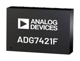
ADG5401FBCPZ-RL7
ActiveFAULT PROTECTION, 6 Ω RON, SPST SWITCH WITH 0.6 KΩ FEEDBACK CHANNEL

ADG5401FBCPZ-RL7
ActiveFAULT PROTECTION, 6 Ω RON, SPST SWITCH WITH 0.6 KΩ FEEDBACK CHANNEL
Description
General part information
ADG5401F Series
The ADG5401F main channel switch is a SPST, low on-resistance switch that features overvoltage protection, power off protection, and overvoltage detection on the source pins (S and SFB). The ADG5401F also features a protected secondary feedback channel for use with digital-to-analog converter (DAC) or amplifier outputs.When no power supplies are present, the switch remains in the off condition, and the switch inputs are high impedance.When powered, if the analog input signal levels on the S pin exceed VDDor VSSby a threshold voltage (VT) the switch turns off, the open-drain FF pin pulls to a logic low and a path between the D and DFB pins is switched on to prevent an open-loop condition on the amplifier output. Input signal levels up to +60 V or −60 V relative to ground are blocked, in both the powered and unpowered condition. The selectable POC pin function allows the protected switch terminal, S, to be connected to GND to minimize glitches on the output. The switch turns on with a Logic 1 input and conducts equally well in both directions. The digital input is compatible with 1.8 V logic inputs over the full operating supply range.Product HighlightsSource pin is protected against voltages greater than the supply rails, up to −60 V and +60 V in both powered and unpowered states.Overvoltage detection with digital output indicates operating state of switches.Trench isolation guards against latch-up.The ADG5401F can operate from a dual supply range of ±5 V to ±22 V or a single-supply range of +8 V to +44 V.Negative channel metal oxide semiconductor (NMOS) only architecture requires 2 V headroom toward VDDand provides low RONand ultraflat RONacross the VSSto VDD− 5 V signal range.ApplicationDAC output protectionAmplifier output protectionAnalog output modulesProcess control/distributed control systemsData acquisitionInstrumentation
Technical Specifications
Parameters and characteristics for this part
| Specification | ADG5401FBCPZ-RL7 |
|---|---|
| -3db Bandwidth | 395 MHz |
| Channel Capacitance (CD(off)) | 11 pF |
| Channel Capacitance (CS(off)) | 9 pF |
| Charge Injection | -230 pC |
| Current - Leakage (Typical) | 100 pA |
| Demultiplexer Outputs | 1 |
| Mounting Type | Surface Mount |
| Multiplexer Inputs | 1 |
| Number of Circuits | 1 |
| On-State Resistance (Typ) | 6 Ohm |
| Operating Temperature (Max) | 125 °C |
| Operating Temperature (Min) | -40 °C |
| Package / Case | 10-WFDFN, CSP |
| Package Length | 3 mm |
| Package Name | 10-LFCSP |
| Package Width | 2 mm |
| Switch Circuit Type | SPST |
| Switch Contact | NC |
| Switch Time Toff (Max) | 360 ns |
| Switch Time Ton (Max) | 10.2 µs |
| Voltage - Supply, Dual (Maximum) | 22 V |
| Voltage - Supply, Dual (Minimum) | -5 V |
| Voltage - Supply, Dual (Nominal) | 5 V |
| Voltage - Supply, Single (V+) (Maximum) | 44 V |
| Voltage - Supply, Single (V+) (Minimum) | 8 V |
Pricing
Prices provided here are for design reference only. For realtime values and availability, please visit the distributors directly
Sign in to see pricing
Create a free account to access distributor pricing data.
CAD
3D models and CAD resources for this part
Documents
Technical documentation and resources