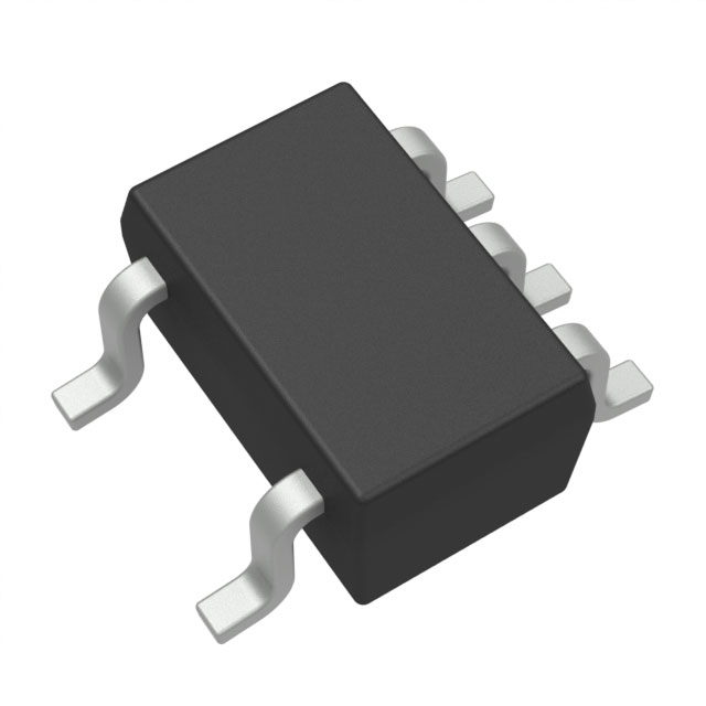
SN74LVC1G00MDCKREP
ActiveENHANCED PRODUCT SINGLE 1-INPUT, 1.65-V TO 5.5-V NAND GATE
Deep-Dive with AI
Search across all available documentation for this part.
SN74LVC1G00MDCKREP
ActiveENHANCED PRODUCT SINGLE 1-INPUT, 1.65-V TO 5.5-V NAND GATE
Deep-Dive with AI
Technical Specifications
Parameters and characteristics commom to parts in this series
| Specification | SN74LVC1G00MDCKREP | SN74LVC1G00-EP Series |
|---|---|---|
| Current - Output High, Low [custom] | 32 mA | 32 mA |
| Current - Output High, Low [custom] | 32 mA | 32 mA |
| Current - Quiescent (Max) [Max] | 10 µA | 10 µA |
| Input Logic Level - High [Max] | 2 V | 2 V |
| Input Logic Level - High [Min] | 1.7 V | 1.7 V |
| Input Logic Level - Low [Max] | 0.8 V | 0.8 V |
| Input Logic Level - Low [Min] | 0.7 V | 0.7 V |
| Logic Type | NAND Gate | NAND Gate |
| Max Propagation Delay @ V, Max CL | 5 ns | 4 - 5 ns |
| Mounting Type | Surface Mount | Surface Mount |
| Number of Circuits | 1 | 1 |
| Number of Inputs | 2 | 2 |
| Operating Temperature [Max] | 125 °C | 85 - 125 °C |
| Operating Temperature [Min] | -55 °C | -55 - -40 °C |
| Package / Case | 5-TSSOP, SOT-353, SC-70-5 | 5-TSSOP, SOT-353, SC-70-5, SOT-753, SC-74A |
| Supplier Device Package | SC-70-5 | SC-70-5, SOT-23-5 |
| Voltage - Supply [Max] | 5.5 V | 5.5 V |
| Voltage - Supply [Min] | 1.65 V | 1.65 V |
Pricing
Prices provided here are for design reference only. For realtime values and availability, please visit the distributors directly
SN74LVC1G00-EP Series
Enhanced product single 1-input, 1.65-V to 5.5-V NAND gate
| Part | Mounting Type | Max Propagation Delay @ V, Max CL | Logic Type | Current - Quiescent (Max) [Max] | Number of Inputs | Input Logic Level - Low [Max] | Input Logic Level - Low [Min] | Voltage - Supply [Max] | Voltage - Supply [Min] | Current - Output High, Low [custom] | Current - Output High, Low [custom] | Input Logic Level - High [Min] | Input Logic Level - High [Max] | Package / Case | Number of Circuits | Operating Temperature [Min] | Operating Temperature [Max] | Supplier Device Package |
|---|---|---|---|---|---|---|---|---|---|---|---|---|---|---|---|---|---|---|
Texas Instruments V62/04732-02XEThis single 2-input positive-NAND gate is designed for 1.65-V to 5.5-V VCCoperation.
The SN74LVC1G00 performs the Boolean function Y =A • Bor Y =A+Bin positive logic.
This device is fully specified for partial-power-down applications using Ioff. The Ioffcircuitry disables the outputs, preventing damaging current backflow through the device when it is powered down.
This single 2-input positive-NAND gate is designed for 1.65-V to 5.5-V VCCoperation.
The SN74LVC1G00 performs the Boolean function Y =A • Bor Y =A+Bin positive logic.
This device is fully specified for partial-power-down applications using Ioff. The Ioffcircuitry disables the outputs, preventing damaging current backflow through the device when it is powered down. | Surface Mount | 5 ns | NAND Gate | 10 µA | 2 | 0.8 V | 0.7 V | 5.5 V | 1.65 V | 32 mA | 32 mA | 1.7 V | 2 V | 5-TSSOP, SC-70-5, SOT-353 | 1 | -55 °C | 125 °C | SC-70-5 |
Texas Instruments SN74LVC1G00IDCKREPThis single 2-input positive-NAND gate is designed for 1.65-V to 5.5-V VCCoperation.
The SN74LVC1G00 performs the Boolean function Y =A • Bor Y =A+Bin positive logic.
This device is fully specified for partial-power-down applications using Ioff. The Ioffcircuitry disables the outputs, preventing damaging current backflow through the device when it is powered down.
This single 2-input positive-NAND gate is designed for 1.65-V to 5.5-V VCCoperation.
The SN74LVC1G00 performs the Boolean function Y =A • Bor Y =A+Bin positive logic.
This device is fully specified for partial-power-down applications using Ioff. The Ioffcircuitry disables the outputs, preventing damaging current backflow through the device when it is powered down. | Surface Mount | 4 ns | NAND Gate | 10 µA | 2 | 0.8 V | 0.7 V | 5.5 V | 1.65 V | 32 mA | 32 mA | 1.7 V | 2 V | 5-TSSOP, SC-70-5, SOT-353 | 1 | -40 °C | 85 °C | SC-70-5 |
Texas Instruments SN74LVC1G00MDBVREPThis single 2-input positive-NAND gate is designed for 1.65-V to 5.5-V VCCoperation.
The SN74LVC1G00 performs the Boolean function Y =A • Bor Y =A+Bin positive logic.
This device is fully specified for partial-power-down applications using Ioff. The Ioffcircuitry disables the outputs, preventing damaging current backflow through the device when it is powered down.
This single 2-input positive-NAND gate is designed for 1.65-V to 5.5-V VCCoperation.
The SN74LVC1G00 performs the Boolean function Y =A • Bor Y =A+Bin positive logic.
This device is fully specified for partial-power-down applications using Ioff. The Ioffcircuitry disables the outputs, preventing damaging current backflow through the device when it is powered down. | Surface Mount | 5 ns | NAND Gate | 10 µA | 2 | 0.8 V | 0.7 V | 5.5 V | 1.65 V | 32 mA | 32 mA | 1.7 V | 2 V | SC-74A, SOT-753 | 1 | -55 °C | 125 °C | SOT-23-5 |
Texas Instruments SN74LVC1G00MDCKREPThis single 2-input positive-NAND gate is designed for 1.65-V to 5.5-V VCCoperation.
The SN74LVC1G00 performs the Boolean function Y =A • Bor Y =A+Bin positive logic.
This device is fully specified for partial-power-down applications using Ioff. The Ioffcircuitry disables the outputs, preventing damaging current backflow through the device when it is powered down.
This single 2-input positive-NAND gate is designed for 1.65-V to 5.5-V VCCoperation.
The SN74LVC1G00 performs the Boolean function Y =A • Bor Y =A+Bin positive logic.
This device is fully specified for partial-power-down applications using Ioff. The Ioffcircuitry disables the outputs, preventing damaging current backflow through the device when it is powered down. | Surface Mount | 5 ns | NAND Gate | 10 µA | 2 | 0.8 V | 0.7 V | 5.5 V | 1.65 V | 32 mA | 32 mA | 1.7 V | 2 V | 5-TSSOP, SC-70-5, SOT-353 | 1 | -55 °C | 125 °C | SC-70-5 |
Description
General part information
SN74LVC1G00-EP Series
This single 2-input positive-NAND gate is designed for 1.65-V to 5.5-V VCCoperation.
The SN74LVC1G00 performs the Boolean function Y =A • Bor Y =A+Bin positive logic.
This device is fully specified for partial-power-down applications using Ioff. The Ioffcircuitry disables the outputs, preventing damaging current backflow through the device when it is powered down.
Documents
Technical documentation and resources