AD537SD/883B
UnknownINTEGRATED CIRCUIT VOLTAGE-TO-FREQUENCY CONVERTER
AD537SD/883B
UnknownINTEGRATED CIRCUIT VOLTAGE-TO-FREQUENCY CONVERTER
Description
General part information
AD537 Series
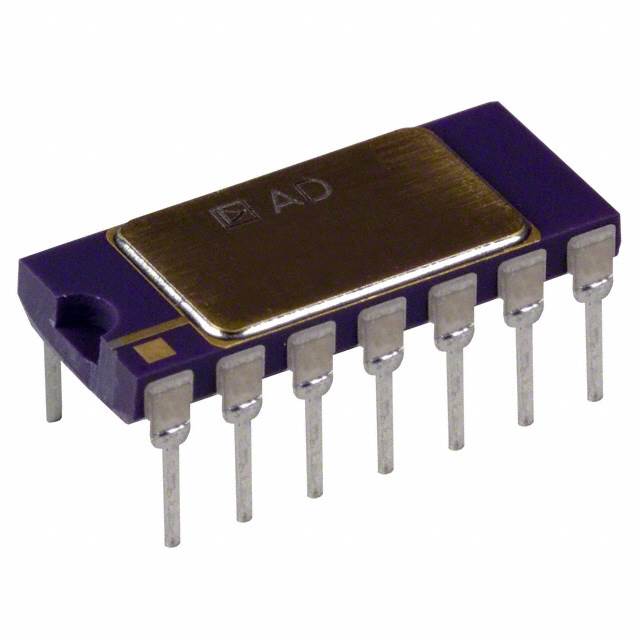
The AD537 is a monolithic V-F converter consisting of an input amplifier, a precision oscillator system, an accurate internal reference generator and a high current output stage. Only a single external RC network is required to set up any full-scale (F.S.) frequency up to 100 kHz and any F.S. input voltage up to ±30 V. Linearity error is as low as ±0.05% for 10 kHz F.S., and operation is guaranteed over an 80 dB dynamic range. The overall temperature coefficient (excluding the effects of external components) is typically ±30 ppm/°C. The AD537 operates from a single supply of 5 V to 36 V and consumes only 1.2 mA quiescent current.A temperature-proportional output, scaled to 1.00 mV/K, enables the circuit to be used as a reliable temperature-to-frequency converter; in combination with the fixed reference output of 1.00 V, offset scales such as 0°C or 0°F can be generated.The low drift (1µV/°C typ) input amplifier allows operation directly from small signals (e.g., thermocouples or strain gages) while offering a high (250 M(Ω) input resistance. Unlike most V-F converters, the AD537 provides a square-wave output, and can drive up to 12 TTL loads, LEDs, very long cables, etc.The excellent temperature characteristics and long-term stability of the AD537 are guaranteed by the primary bandgap reference generator and the low T.C. silicon chromium thin film resistors used throughout.The device is available in either a TO-116 ceramic DIP or a TO-100 metal can; both are hermetically sealed packages.The AD537 is available in three performance/temperature grades; the J and K grades are specified for operation over the 0°C to +70°C range while the AD537S is specified for operation over the extended temperature range, -55°C to +125°C.PRODUCT HIGHLIGHTSThe AD537 is a complete V-F converter requiring only an external RC timing network to set the desired full-scale frequency and a selectable pull-up resistor for the open collector output stage. Any full-scale input voltage range from 100 mV to 10 volts (or greater, depending on +VS) can be accommodated by proper selection of timing resistor. The full-scale frequency is then set by the timing capacitor from the simple relationship, f = V/10RC.The power supply requirements are minimal, only 1.2 mA quiescent current is drawn from a single positive supply from 4.5 volts to 36 volts. In this mode, positive inputs can vary from 0 volts (ground) to (+Vs - 4) volts. Negative inputs can easily be connected for below ground operation.F-V converters with excellent characteristic are also easy to build by connecting the AD537 in a phase-locked loop. Application particulars are shown in Figure 6.The versatile open-collector NPN output stage can sink up to 20 mA with a saturation voltage less than 0.4 volts. The Logic Common terminal can be connected to any level between ground (or -V) and 4 volts below +Vs. This allows easy direct interface to any logic family with either positive or negative logic levels.The AD537 is available in versions compliant with MIL STD-883. Refer to the Analog Devices Military Product Databook or current AD537/883B data sheet for detailed specifications.
Technical Specifications
Parameters and characteristics for this part
| Specification | AD537SD/883B |
|---|---|
| Frequency - Max | 100 kHz |
| Full Scale | 30 ppm/°C |
| Linearity Tolerance | 0.05 % |
| Mounting Type | Through Hole |
| Package Length | 0.3 in |
| Package Name | 14-CDIP |
| Package Width | 7.62 mm |
| Type | Voltage to Frequency |
Pricing
Prices provided here are for design reference only. For realtime values and availability, please visit the distributors directly
Sign in to see pricing
Create a free account to access distributor pricing data.
CAD
3D models and CAD resources for this part
Documents
Technical documentation and resources