ADC10040CIMTX/NOPB
Active10-BIT, 40-MSPS ANALOG-TO-DIGITAL CONVERTER (ADC)
Deep-Dive with AI
Search across all available documentation for this part.
ADC10040CIMTX/NOPB
Active10-BIT, 40-MSPS ANALOG-TO-DIGITAL CONVERTER (ADC)
Deep-Dive with AI
Technical Specifications
Parameters and characteristics commom to parts in this series
| Specification | ADC10040CIMTX/NOPB | ADC10040 Series |
|---|---|---|
| Architecture | Pipelined | Pipelined |
| Configuration | S/H-ADC | S/H-ADC |
| Data Interface | Parallel | Parallel |
| Grade | - | Automotive |
| Input Type | Differential, Single Ended | Differential, Single Ended |
| Mounting Type | Surface Mount | Surface Mount |
| Number of A/D Converters | 1 | 1 |
| Number of Bits | 10 | 10 |
| Number of Inputs | 1 | 1 |
| Operating Temperature [Max] | 85 °C | 85 °C |
| Operating Temperature [Min] | -40 °C | -40 °C |
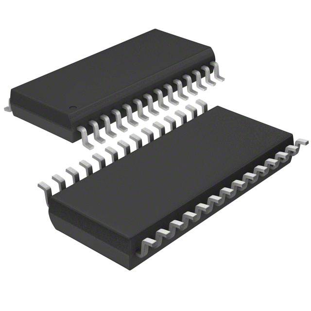
| Package / Case | 28-TSSOP | 28-TSSOP |
| Package / Case | 4.4 mm | 4.4 mm |
| Package / Case | 0.173 in | 0.173 in |
| Qualification | - | AEC-Q100 |
| Ratio - S/H:ADC | 1:1 | 1:1 |
| Reference Type | Internal, External | Internal, External |
| Sampling Rate (Per Second) | 40 M | 40 M |
| Supplier Device Package | 28-TSSOP | 28-TSSOP |
| Voltage - Supply, Analog [Max] | 3.6 V | 3.6 V |
| Voltage - Supply, Analog [Min] | 2.7 V | 2.7 V |
| Voltage - Supply, Digital [Max] | 3.6 V | 3.6 V |
| Voltage - Supply, Digital [Min] | 2.5 V | 2.5 V |
Pricing
Prices provided here are for design reference only. For realtime values and availability, please visit the distributors directly
ADC10040 Series
10-Bit, 40-MSPS Analog-to-Digital Converter (ADC)
| Part | Input Type | Number of Inputs | Number of A/D Converters | Data Interface | Configuration | Package / Case | Package / Case | Package / Case | Reference Type | Sampling Rate (Per Second) | Operating Temperature [Min] | Operating Temperature [Max] | Voltage - Supply, Digital [Max] | Voltage - Supply, Digital [Min] | Ratio - S/H:ADC | Mounting Type | Supplier Device Package | Architecture | Number of Bits | Voltage - Supply, Analog [Min] | Voltage - Supply, Analog [Max] | Qualification | Grade |
|---|---|---|---|---|---|---|---|---|---|---|---|---|---|---|---|---|---|---|---|---|---|---|---|
Texas Instruments ADC10040CIMT/NOPBThe ADC10040 is a monolithic CMOS analog-to-digital converter capable of converting analog input signals into 10-bit digital words at 40 Megasamples per second (MSPS). This converter uses a differential, pipeline architecture with digital error correction and an on-chip sample-and-hold circuit to provide a complete conversion solution, and to minimize power consumption, while providing excellent dynamic performance. A unique sample-and-hold stage yields a full-power bandwidth of 400 MHz. Operating on a single 3.0V power supply, this device consumes just 55.5 mW at 40 MSPS, including the reference current. The Standby feature reduces power consumption to just 13.5 mW.
The differential inputs provide a full scale selectable input swing of 2.0 VP-P, 1.5 VP-P, 1.0 VP-P, with the possibility of a single-ended input. Full use of the differential input is recommended for optimum performance. An internal +1.2V precision bandgap reference is used to set the ADC full-scale range, and also allows the user to supply a buffered referenced voltage for those applications requiring increased accuracy. The output data format is user choice of offset binary or two’s complement.
The ADC10040Q runs on an Automotive Grade Flow and is AEC-Q100 Grade 3 Qualified.
This device is available in the 28-lead TSSOP package and will operate over the industrial temperature range of −40°C to +85°C.
The ADC10040 is a monolithic CMOS analog-to-digital converter capable of converting analog input signals into 10-bit digital words at 40 Megasamples per second (MSPS). This converter uses a differential, pipeline architecture with digital error correction and an on-chip sample-and-hold circuit to provide a complete conversion solution, and to minimize power consumption, while providing excellent dynamic performance. A unique sample-and-hold stage yields a full-power bandwidth of 400 MHz. Operating on a single 3.0V power supply, this device consumes just 55.5 mW at 40 MSPS, including the reference current. The Standby feature reduces power consumption to just 13.5 mW.
The differential inputs provide a full scale selectable input swing of 2.0 VP-P, 1.5 VP-P, 1.0 VP-P, with the possibility of a single-ended input. Full use of the differential input is recommended for optimum performance. An internal +1.2V precision bandgap reference is used to set the ADC full-scale range, and also allows the user to supply a buffered referenced voltage for those applications requiring increased accuracy. The output data format is user choice of offset binary or two’s complement.
The ADC10040Q runs on an Automotive Grade Flow and is AEC-Q100 Grade 3 Qualified.
This device is available in the 28-lead TSSOP package and will operate over the industrial temperature range of −40°C to +85°C. | Differential, Single Ended | 1 | 1 | Parallel | S/H-ADC | 28-TSSOP | 4.4 mm | 0.173 in | External, Internal | 40 M | -40 °C | 85 °C | 3.6 V | 2.5 V | 1:1 | Surface Mount | 28-TSSOP | Pipelined | 10 | 2.7 V | 3.6 V | ||
Texas Instruments ADC10040QCIMTX/NOPBThe ADC10040 is a monolithic CMOS analog-to-digital converter capable of converting analog input signals into 10-bit digital words at 40 Megasamples per second (MSPS). This converter uses a differential, pipeline architecture with digital error correction and an on-chip sample-and-hold circuit to provide a complete conversion solution, and to minimize power consumption, while providing excellent dynamic performance. A unique sample-and-hold stage yields a full-power bandwidth of 400 MHz. Operating on a single 3.0V power supply, this device consumes just 55.5 mW at 40 MSPS, including the reference current. The Standby feature reduces power consumption to just 13.5 mW.
The differential inputs provide a full scale selectable input swing of 2.0 VP-P, 1.5 VP-P, 1.0 VP-P, with the possibility of a single-ended input. Full use of the differential input is recommended for optimum performance. An internal +1.2V precision bandgap reference is used to set the ADC full-scale range, and also allows the user to supply a buffered referenced voltage for those applications requiring increased accuracy. The output data format is user choice of offset binary or two’s complement.
The ADC10040Q runs on an Automotive Grade Flow and is AEC-Q100 Grade 3 Qualified.
This device is available in the 28-lead TSSOP package and will operate over the industrial temperature range of −40°C to +85°C.
The ADC10040 is a monolithic CMOS analog-to-digital converter capable of converting analog input signals into 10-bit digital words at 40 Megasamples per second (MSPS). This converter uses a differential, pipeline architecture with digital error correction and an on-chip sample-and-hold circuit to provide a complete conversion solution, and to minimize power consumption, while providing excellent dynamic performance. A unique sample-and-hold stage yields a full-power bandwidth of 400 MHz. Operating on a single 3.0V power supply, this device consumes just 55.5 mW at 40 MSPS, including the reference current. The Standby feature reduces power consumption to just 13.5 mW.
The differential inputs provide a full scale selectable input swing of 2.0 VP-P, 1.5 VP-P, 1.0 VP-P, with the possibility of a single-ended input. Full use of the differential input is recommended for optimum performance. An internal +1.2V precision bandgap reference is used to set the ADC full-scale range, and also allows the user to supply a buffered referenced voltage for those applications requiring increased accuracy. The output data format is user choice of offset binary or two’s complement.
The ADC10040Q runs on an Automotive Grade Flow and is AEC-Q100 Grade 3 Qualified.
This device is available in the 28-lead TSSOP package and will operate over the industrial temperature range of −40°C to +85°C. | Differential, Single Ended | 1 | 1 | Parallel | S/H-ADC | 28-TSSOP | 4.4 mm | 0.173 in | External, Internal | 40 M | -40 °C | 85 °C | 3.6 V | 2.5 V | 1:1 | Surface Mount | 28-TSSOP | Pipelined | 10 | 2.7 V | 3.6 V | AEC-Q100 | Automotive |
Texas Instruments ADC10040QCIMT/NOPBThe ADC10040 is a monolithic CMOS analog-to-digital converter capable of converting analog input signals into 10-bit digital words at 40 Megasamples per second (MSPS). This converter uses a differential, pipeline architecture with digital error correction and an on-chip sample-and-hold circuit to provide a complete conversion solution, and to minimize power consumption, while providing excellent dynamic performance. A unique sample-and-hold stage yields a full-power bandwidth of 400 MHz. Operating on a single 3.0V power supply, this device consumes just 55.5 mW at 40 MSPS, including the reference current. The Standby feature reduces power consumption to just 13.5 mW.
The differential inputs provide a full scale selectable input swing of 2.0 VP-P, 1.5 VP-P, 1.0 VP-P, with the possibility of a single-ended input. Full use of the differential input is recommended for optimum performance. An internal +1.2V precision bandgap reference is used to set the ADC full-scale range, and also allows the user to supply a buffered referenced voltage for those applications requiring increased accuracy. The output data format is user choice of offset binary or two’s complement.
The ADC10040Q runs on an Automotive Grade Flow and is AEC-Q100 Grade 3 Qualified.
This device is available in the 28-lead TSSOP package and will operate over the industrial temperature range of −40°C to +85°C.
The ADC10040 is a monolithic CMOS analog-to-digital converter capable of converting analog input signals into 10-bit digital words at 40 Megasamples per second (MSPS). This converter uses a differential, pipeline architecture with digital error correction and an on-chip sample-and-hold circuit to provide a complete conversion solution, and to minimize power consumption, while providing excellent dynamic performance. A unique sample-and-hold stage yields a full-power bandwidth of 400 MHz. Operating on a single 3.0V power supply, this device consumes just 55.5 mW at 40 MSPS, including the reference current. The Standby feature reduces power consumption to just 13.5 mW.
The differential inputs provide a full scale selectable input swing of 2.0 VP-P, 1.5 VP-P, 1.0 VP-P, with the possibility of a single-ended input. Full use of the differential input is recommended for optimum performance. An internal +1.2V precision bandgap reference is used to set the ADC full-scale range, and also allows the user to supply a buffered referenced voltage for those applications requiring increased accuracy. The output data format is user choice of offset binary or two’s complement.
The ADC10040Q runs on an Automotive Grade Flow and is AEC-Q100 Grade 3 Qualified.
This device is available in the 28-lead TSSOP package and will operate over the industrial temperature range of −40°C to +85°C. | Differential, Single Ended | 1 | 1 | Parallel | S/H-ADC | 28-TSSOP | 4.4 mm | 0.173 in | External, Internal | 40 M | -40 °C | 85 °C | 3.6 V | 2.5 V | 1:1 | Surface Mount | 28-TSSOP | Pipelined | 10 | 2.7 V | 3.6 V | AEC-Q100 | Automotive |
Texas Instruments ADC10040CIMTX/NOPBThe ADC10040 is a monolithic CMOS analog-to-digital converter capable of converting analog input signals into 10-bit digital words at 40 Megasamples per second (MSPS). This converter uses a differential, pipeline architecture with digital error correction and an on-chip sample-and-hold circuit to provide a complete conversion solution, and to minimize power consumption, while providing excellent dynamic performance. A unique sample-and-hold stage yields a full-power bandwidth of 400 MHz. Operating on a single 3.0V power supply, this device consumes just 55.5 mW at 40 MSPS, including the reference current. The Standby feature reduces power consumption to just 13.5 mW.
The differential inputs provide a full scale selectable input swing of 2.0 VP-P, 1.5 VP-P, 1.0 VP-P, with the possibility of a single-ended input. Full use of the differential input is recommended for optimum performance. An internal +1.2V precision bandgap reference is used to set the ADC full-scale range, and also allows the user to supply a buffered referenced voltage for those applications requiring increased accuracy. The output data format is user choice of offset binary or two’s complement.
The ADC10040Q runs on an Automotive Grade Flow and is AEC-Q100 Grade 3 Qualified.
This device is available in the 28-lead TSSOP package and will operate over the industrial temperature range of −40°C to +85°C.
The ADC10040 is a monolithic CMOS analog-to-digital converter capable of converting analog input signals into 10-bit digital words at 40 Megasamples per second (MSPS). This converter uses a differential, pipeline architecture with digital error correction and an on-chip sample-and-hold circuit to provide a complete conversion solution, and to minimize power consumption, while providing excellent dynamic performance. A unique sample-and-hold stage yields a full-power bandwidth of 400 MHz. Operating on a single 3.0V power supply, this device consumes just 55.5 mW at 40 MSPS, including the reference current. The Standby feature reduces power consumption to just 13.5 mW.
The differential inputs provide a full scale selectable input swing of 2.0 VP-P, 1.5 VP-P, 1.0 VP-P, with the possibility of a single-ended input. Full use of the differential input is recommended for optimum performance. An internal +1.2V precision bandgap reference is used to set the ADC full-scale range, and also allows the user to supply a buffered referenced voltage for those applications requiring increased accuracy. The output data format is user choice of offset binary or two’s complement.
The ADC10040Q runs on an Automotive Grade Flow and is AEC-Q100 Grade 3 Qualified.
This device is available in the 28-lead TSSOP package and will operate over the industrial temperature range of −40°C to +85°C. | Differential, Single Ended | 1 | 1 | Parallel | S/H-ADC | 28-TSSOP | 4.4 mm | 0.173 in | External, Internal | 40 M | -40 °C | 85 °C | 3.6 V | 2.5 V | 1:1 | Surface Mount | 28-TSSOP | Pipelined | 10 | 2.7 V | 3.6 V |
Description
General part information
ADC10040 Series
The ADC10040 is a monolithic CMOS analog-to-digital converter capable of converting analog input signals into 10-bit digital words at 40 Megasamples per second (MSPS). This converter uses a differential, pipeline architecture with digital error correction and an on-chip sample-and-hold circuit to provide a complete conversion solution, and to minimize power consumption, while providing excellent dynamic performance. A unique sample-and-hold stage yields a full-power bandwidth of 400 MHz. Operating on a single 3.0V power supply, this device consumes just 55.5 mW at 40 MSPS, including the reference current. The Standby feature reduces power consumption to just 13.5 mW.
The differential inputs provide a full scale selectable input swing of 2.0 VP-P, 1.5 VP-P, 1.0 VP-P, with the possibility of a single-ended input. Full use of the differential input is recommended for optimum performance. An internal +1.2V precision bandgap reference is used to set the ADC full-scale range, and also allows the user to supply a buffered referenced voltage for those applications requiring increased accuracy. The output data format is user choice of offset binary or two’s complement.
The ADC10040Q runs on an Automotive Grade Flow and is AEC-Q100 Grade 3 Qualified.
Documents
Technical documentation and resources