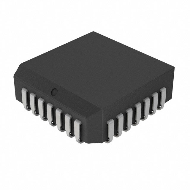
74FCT388915TDJG
ObsoleteIC PLL CLOCK DRIVER 28PLCC
74FCT388915TDJG
ObsoleteIC PLL CLOCK DRIVER 28PLCC
Description
General part information
74FCT388915T Series
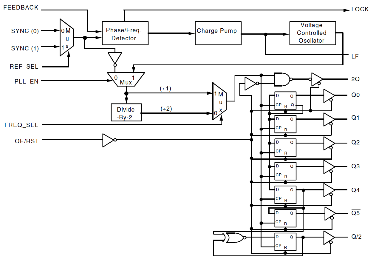
The FCT388915T uses phase-lock loop technology to lock the frequency and phase of outputs to the input reference clock. It provides low skew clock distribution for high performance PCs and workstations. One of the outputs is fed back to the PLL at the FEEDBACK input resulting in essentially zero delay across the device. The PLL consists of the phase/ frequency detector, charge pump, loop filter and VCO. The VCO is designed for a 2Q operating frequency range of 40MHz to f2Q Max. The FCT388915T provides 8 outputs, the Q5 output is inverted from the Q outputs. The 2Q runs at twice the Q frequency and Q/2 runs at half the Q frequency. The FREQ_SEL control provides an additional ÷ 2 option in the output path. PLL _EN allows bypassing of the PLL, which is useful in static test modes. When PLL_EN is low, SYNC input may be used as a test clock. In this test mode, the input frequency is not limited to the specified range and the polarity of outputs is complementary to that in normal operation (PLL_EN = 1). The LOCK output attains logic HIGH when the PLL is in steady-state phase and frequency lock. When OE/RST is low, all the outputs are put in high impedance state and registers at Q, Q and Q/2 outputs are reset. The FCT388915T requires one external loop filter component as recommended in Figure 3.
Technical Specifications
Parameters and characteristics for this part
| Specification | 74FCT388915TDJG |
|---|---|
| Differential Input | No |
| Differential Output | No |
| Divider | Yes |
| Frequency - Max | 133 MHz |
| Input | LVTTL |
| Input Ratio | 2 |
| Mounting Type | Surface Mount |
| Multiplier | Yes |
| Number of Circuits | 1 |
| Operating Temperature (Max) | 70 °C |
| Operating Temperature (Min) | 0 °C |
| Output | LVTTL, LVCMOS |
| Output Ratio | 8 |
| Package / Case | 28-LCC (J-Lead) |
| Package Length | 11.51 mm |
| Package Name | 28-PLCC |
| Package Width | 11.51 mm |
| PLL | Yes with Bypass |
| Type | PLL Clock Driver |
| Voltage - Supply (Maximum) | 3.6 V |
| Voltage - Supply (Minimum) | 3 V |
Pricing
Prices provided here are for design reference only. For realtime values and availability, please visit the distributors directly
Sign in to see pricing
Create a free account to access distributor pricing data.
CAD
3D models and CAD resources for this part
Documents
Technical documentation and resources