


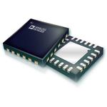
ADGS1212BCPZ
ActiveANALOG SWITCH ICS SPI INTERFACE, QUAD SPST SWITCH, LOW QINJ, LOW CON, 15 V/+12 V, MUX CONFIGURABLE

ADGS1212BCPZ
ActiveANALOG SWITCH ICS SPI INTERFACE, QUAD SPST SWITCH, LOW QINJ, LOW CON, 15 V/+12 V, MUX CONFIGURABLE
Description
General part information
ADGS1212 Series
The ADGS1212 contains four independent single-pole/single-throw (SPST) switches. A serial peripheral interface (SPI) controls the switches. The SPI interface has robust error detection features such as cyclic redundancy check (CRC) error detection, invalid read/write address detection, and SCLK count error detection.It is possible to daisy-chain multiple ADGS1212 devices together. Daisy-chain mode enables the configuration of multiple devices with minimal digital lines. The ADGS1212 can also operate in burst mode to decrease the time between SPI commands.iCMOS construction ensures ultralow power dissipation, making the device ideal for portable and battery-powered instruments.Each switch conducts equally well in both directions when on, and each switch has an input signal range that extends to the supplies.In the off condition, signal levels up to the supplies are blocked. The ultralow capacitance and charge injection of these switches make them ideal solutions for data acquisition and sample-andhold applications where low glitch and fast settling are required.Fast switching speed coupled with high signal bandwidth make the device suitable for video signal switching.Multifunction pin names may be referenced by their relevant function only.Product HighlightsSPI interface removes the need for parallel conversion, logic traces, and reduces the general-purpose input/output (GPIO) channel count.Daisy-chain mode removes additional logic traces when multiple devices are used.CRC error detection, invalid read/write address detection, and SCLK count error detection ensure a robust digital interface.CRC and error detection capabilities allow the ADGS1212 to be used in safety critical systems.Guaranteed break-before-make switching allows the the ADGS1212 to be used in multiplexer configurations with external wiring.The ADGS1212 1.8 V logic compatibility with 2.7 V ≤ VL≤ 3.3 VUltralow capacitance.<1 pC charge injection.ApplicationsAutomated test equipmentData acquisition systemsBattery-powered systemsSample-and-hold systemsAudio signal routingVideo signal routingCommunications systems
Technical Specifications
Parameters and characteristics for this part
| Specification | ADGS1212BCPZ |
|---|---|
| -3db Bandwidth | 1 GHz |
| Channel Capacitance (CD(off)) | 1.5 pF |
| Channel Capacitance (CS(off)) | 1.4 pF |
| Channel-to-Channel Matching (ΔRon) (Option 1) | 11 Ohm |
| Channel-to-Channel Matching (ΔRon) (Option 2) | 27 Ohm |
| Charge Injection | 1 pC |
| Crosstalk | -110 dB |
| Current - Leakage (Max) | 1 nA |
| Demultiplexer Outputs | 1 |
| Mounting Type | Surface Mount |
| Multiplexer Inputs | 1 |
| Number of Circuits | 4 |
| On-State Resistance (Max) | 260 Ohms, 625 Ohm |
| Operating Temperature (Max) | 125 °C |
| Operating Temperature (Min) | -40 °C |
| Package / Case | CSP, 24-WFQFN Exposed Pad |
| Package Length | 4 mm |
| Package Name | 24-LFCSP |
| Package Width | 4 mm |
| Switch Circuit Type | SPST |
| Switch Contact | NO |
| Switch Time Toff (Max) | 225 ns |
| Switch Time Ton (Max) | 490 ns |
| Voltage - Supply, Dual (Maximum) | 16.5 V |
| Voltage - Supply, Dual (Minimum) | -4.5 V |
| Voltage - Supply, Dual (Nominal) | 4.5 V |
| Voltage - Supply, Single (V+) (Maximum) | 16.5 V |
| Voltage - Supply, Single (V+) (Minimum) | 5 V |
Pricing
Prices provided here are for design reference only. For realtime values and availability, please visit the distributors directly
Sign in to see pricing
Create a free account to access distributor pricing data.
CAD
3D models and CAD resources for this part
Documents
Technical documentation and resources