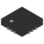
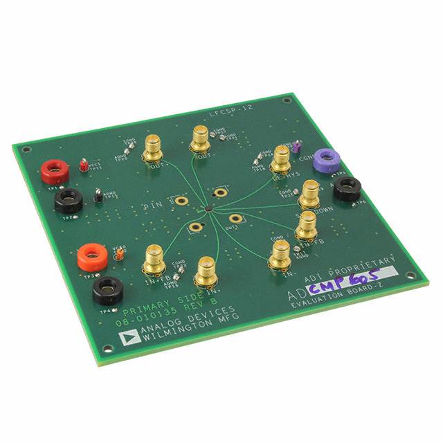
ADCMP605BCPZ-R2
UnknownIC COMPARATOR 1 W/LATCH 12LFCSP
ADCMP605BCPZ-R2
UnknownIC COMPARATOR 1 W/LATCH 12LFCSP
Description
General part information
ADCMP605 Series
TheADCMP604/ ADCMP605 are very fast comparators fabricated on the Analog Devices, Inc. proprietary XFCB2 process. These comparators are exceptionally versatile and easy to use. Features include an input range from VEE− 0.5 V to VCCI+ 0.2 V, low noise, LVDS-compatible output drivers, and TTL/CMOS latch inputs with adjustable hysteresis and/or shut-down inputs.The devices offer 1.5 ns propagation delays with 1 ps rms random jitter (RJ). Overdrive and slew rate dispersion are typically less than 50 ps. A flexible power supply scheme allows the devices to operate with a single 2.5 V positive supply and a −0.5 V to +2.7 V input signal range up to a 5.5 V positive supply with a −0.5 V to +5.7 V input signal range. Split input/output supplies, with no sequencing restrictions on the ADCMP605, support a wide input signal range with greatly reduced power consumption.The LVDS-compatible output stage is designed to drive any standard LVDS input. The comparator input stage offers robust protection against large input overdrive, and the outputs do not phase reverse when the valid input signal range is exceeded. High speed latch and programmable hysteresis features are also provided in a unique single-pin control option.The ADCMP604 is available in a 6-lead SC70 package, and the ADCMP605 is available in a 12-lead LFCSP.APPLICATIONSHigh speed instrumentationClock and data signal restorationLogic level shifting or translationPulse spectroscopyHigh speed line receiversThreshold detectionPeak and zero-crossing detectorsHigh speed trigger circuitryPulse-width modulatorsCurrent-/voltage-controlled oscillatorsAutomatic test equipment (ATE)
Technical Specifications
Parameters and characteristics for this part
| Specification | ADCMP605BCPZ-R2 |
|---|---|
| CMRR (Typ) | 50 dB |
| Current - Input Bias (Max) | 5 µA |
| Current - Output (Typ) | 50 mA |
| Current - Quiescent (Max) | 3 mA |
| Hysteresis | 100 µV |
| Mounting Type | Surface Mount |
| Number of Elements | 1 |
| Operating Temperature (Max) | 125 °C |
| Operating Temperature (Min) | -40 °C |
| Output Type | LVDS, Complementary, Rail-to-Rail |
| Package / Case | CSP, 12-WFQFN Exposed Pad |
| Package Length | 3 mm |
| Package Name | 12-LFCSP |
| Package Width | 3 mm |
| Propagation Delay (Max) | 3 ns |
| PSRR (Typ) | 50 dB |
| Supply Configuration | Dual, Single |
| Type | with Latch |
| Voltage - Input Offset (Max) | 5 mV |
| Voltage - Supply (Single) Maximum | 5.5 V |
| Voltage - Supply (Single) Minimum | 2.5 V |
Pricing
Prices provided here are for design reference only. For realtime values and availability, please visit the distributors directly
Sign in to see pricing
Create a free account to access distributor pricing data.
CAD
3D models and CAD resources for this part
Documents
Technical documentation and resources