MAX5308EUE+
ActiveLOW-POWER, LOW-GLITCH, OCTAL 10-BIT VOLTAGE-OUTPUT DACS WITH SERIAL INTERFACE
MAX5308EUE+
ActiveLOW-POWER, LOW-GLITCH, OCTAL 10-BIT VOLTAGE-OUTPUT DACS WITH SERIAL INTERFACE
Description
General part information
MAX5308 Series
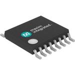
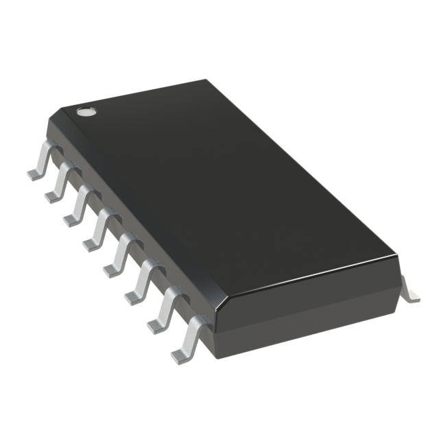
The MAX5308/MAX5309 are 10-bit, eight channel, low-power, voltage-output, digital-to-analog converters (DACs) in a space-saving 16-pin TSSOP package. The wide +2.7V to +5.5V supply voltage range and less than 215µA (max) supply current per DAC are excellent for low-power and low-voltage applications. The low 2nV-s glitch energy of the MAX5308/MAX5309 makes them ideal for digital control of fast-response, closed-loop systems.The MAX5308 has a digital output (DOUT) that can be used for daisy-chaining multiple devices. The MAX5309 has a hardware reset input (active-low CLR) which clears all registers and DACs to zero. The MAX5308/MAX5309 have a software shutdown feature that reduces the supply current to 1µA. The MAX5308/MAX5309 feature a load DAC (active-low LDAC) function that updates the output of all eight DACs simultaneously.The 3-wire SPI™, QSPI™, MICROWIRE™ and DSP-compatible serial interface allows the input and DAC registers to be updated independently or simultaneously with a single software command. These devices use a double-buffered design to minimize the digital-noise feedthrough from the digital inputs to the outputs. The MAX5308/MAX5309 operating temperature range is from -40°C to +85°C.ApplicationsControl of Optical ComponentsGain and Offset AdjustmentPortable Instrumentation EquipmentPower Amplifier ControlProcess-Control I/O Boards
Technical Specifications
Parameters and characteristics for this part
| Specification | MAX5308EUE+ |
|---|---|
| Data Interface | DSP, SPI |
| Differential Output | No |
| DNL (LSB) Tolerance | 0.5 LSB, 0.5 LSB |
| INL (LSB) Tolerance | 0.5 LSB |
| INL (Max) (LSB) | 0.5 LSB |
| Mounting Type | Surface Mount |
| Number of Bits | 10 bits |
| Number of D/A Converters | 8 count |
| Operating Temperature (Max) | 85 °C |
| Operating Temperature (Min) | -40 °C |
| Output Type | Voltage - Buffered |
| Package Length | 0.173 in |
| Package Name | 16-TSSOP |
| Package Width | 4.4 mm |
| Reference Type | External |
| Settling Time (Typical) | 5 µs |
| Voltage - Supply, Analog (Max) | 5.5 V |
| Voltage - Supply, Analog (Min) | 2.7 V |
| Voltage - Supply, Digital (Max) | 5.5 V |
| Voltage - Supply, Digital (Min) | 2.7 V |
Pricing
Prices provided here are for design reference only. For realtime values and availability, please visit the distributors directly
Sign in to see pricing
Create a free account to access distributor pricing data.
CAD
3D models and CAD resources for this part