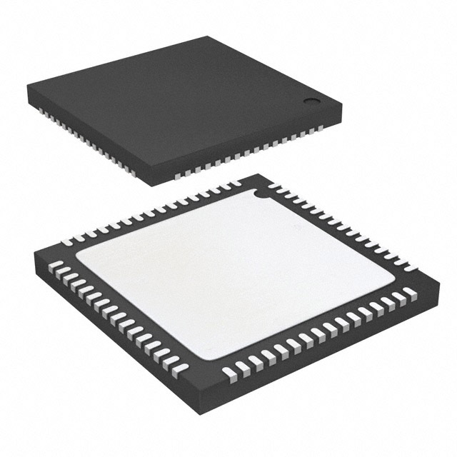
AD9212ABCPZ-40
ActiveOCTAL, 10-BIT, 40 MSPS/65 MSPS, SERIAL LVDS, 1.8 V ADC
AD9212ABCPZ-40
ActiveOCTAL, 10-BIT, 40 MSPS/65 MSPS, SERIAL LVDS, 1.8 V ADC
Description
General part information
AD9212 Series
The AD9212 is an octal, 10-bit, 40 MSPS/65 MSPS ADC with an on-chip sample-and-hold circuit designed for low cost, low power, small size, and ease of use. Operating at a conversion rate of up to 65 MSPS, it is optimized for outstanding dynamic performance and low power in applications where a small package size is critical.The ADC requires a single 1.8 V power supply and LVPECL-/ CMOS-/LVDS-compatible sample rate clock for full performance operation. No external reference or driver components are required for many applications.The ADC automatically multiplies the sample rate clock for the appropriate LVDS serial data rate. A data clock (DCO) for capturing data on the output and a frame clock (FCO) for signaling a new output byte are provided. Individual channel power-down is supported and typically consumes less than 2 mW when all channels are disabled.The ADC contains several features designed to maximize flexibility and minimize system cost, such as programmable clock and data alignment and programmable digital test pattern generation. The available digital test patterns include built-in deterministic and pseudorandom patterns, along with custom user- defined test patterns entered via the serial port interface (SPI).The AD9212 is available in a RoHS-compliant, 64-lead LFCSP. It is specified over the industrial temperature range of −40°C to +85°C.PRODUCT HIGHLIGHTSSmall Footprint. Eight ADCs are contained in a small package.Low Power of 100 mW per Channel at 65 MSPS.Ease of Use. A data clock output (DCO) operates up to 300 MHz and supports double data rate (DDR) operation.User Flexibility. SPI control offers a wide range of flexible features to meet specific system requirements.Pin-Compatible Family. This includes theAD9222(12-bit) andAD9252(14-bit).APPLICATIONSMedical imaging and nondestructive ultrasoundPortable ultrasound and digital beam-forming systemsQuadrature radio receiversDiversity radio receiversTape drivesOptical networkingTest equipment
Technical Specifications
Parameters and characteristics for this part
| Specification | AD9212ABCPZ-40 |
|---|---|
| Architecture | Pipelined |
| Configuration | S/H-ADC |
| Data Interface | LVDS - Serial |
| Features | Simultaneous Sampling |
| Input Type | Single Ended, Differential |
| Mounting Type | Surface Mount |
| Number of A/D Converters | 8 count |
| Number of Bits | 10 bits |
| Number of Inputs | 8 |
| Operating Temperature (Max) | 85 °C |
| Operating Temperature (Min) | -40 °C |
| Package / Case | CSP, 64-VFQFN Exposed Pad |
| Package Length | 9 mm |
| Package Name | 64-LFCSP-VQ |
| Package Width | 9 mm |
| Ratio - ADC | 1 |
| Ratio - S/H | 1 |
| Reference Type | Internal |
| Sampling Rate (Per Second) | 40 MHz |
| Voltage - Supply, Analog (Max) | 1.9 V |
| Voltage - Supply, Analog (Min) | 1.7 V |
| Voltage - Supply, Digital (Max) | 1.9 V |
| Voltage - Supply, Digital (Min) | 1.7 V |
Pricing
Prices provided here are for design reference only. For realtime values and availability, please visit the distributors directly
Sign in to see pricing
Create a free account to access distributor pricing data.
CAD
3D models and CAD resources for this part
Documents
Technical documentation and resources