CSD97395Q4MT
ActiveCSD97395Q4M HIGH FREQUENCY SYNCHRONOUS BUCK NEXFET™ POWER STAGE
Deep-Dive with AI
Search across all available documentation for this part.
CSD97395Q4MT
ActiveCSD97395Q4M HIGH FREQUENCY SYNCHRONOUS BUCK NEXFET™ POWER STAGE
Technical Specifications
Parameters and characteristics commom to parts in this series
| Specification | CSD97395Q4MT | CSD97395 Series |
|---|---|---|
| Applications | Synchronous Buck Converters | Synchronous Buck Converters |
| Current - Output / Channel | 25 A | 25 A |
| Current - Peak Output | 60 A | 60 A |
| Fault Protection | Shoot-Through, UVLO | Shoot-Through, UVLO |
| Features | Bootstrap Circuit | Bootstrap Circuit |
| Interface | PWM | PWM |
| Load Type | Inductive | Inductive |
| Mounting Type | Surface Mount | Surface Mount |
| Operating Temperature [Max] | 150 C | 150 C |
| Operating Temperature [Min] | -40 °C | -40 °C |
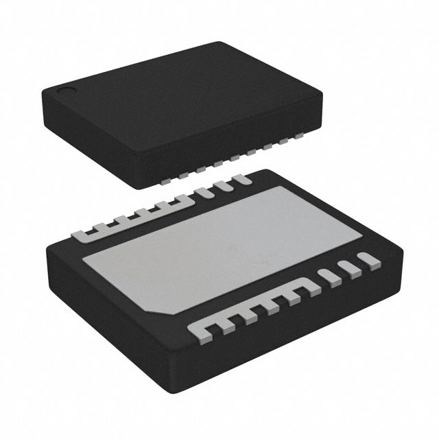
| Package / Case | 8-PowerVFDFN | 8-PowerVFDFN |
| Supplier Device Package | 8-VSON (3.5x4.5) | 8-VSON (3.5x4.5) |
| Technology | Power MOSFET | Power MOSFET |
| Voltage - Load [Max] | 24 V | 24 V |
| Voltage - Load [Min] | 4.5 V | 4.5 V |
| Voltage - Supply [Max] | 5.5 V | 5.5 V |
| Voltage - Supply [Min] | 4.5 V | 4.5 V |
Pricing
Prices provided here are for design reference only. For realtime values and availability, please visit the distributors directly
| Distributor | Package | Quantity | $ | |
|---|---|---|---|---|
| Digikey | Cut Tape (CT) | 1 | $ 2.54 | |
| 10 | $ 2.29 | |||
| 25 | $ 2.16 | |||
| 100 | $ 1.84 | |||
| Digi-Reel® | 1 | $ 2.54 | ||
| 10 | $ 2.29 | |||
| 25 | $ 2.16 | |||
| 100 | $ 1.84 | |||
| Tape & Reel (TR) | 250 | $ 1.73 | ||
| 500 | $ 1.51 | |||
| 1250 | $ 1.25 | |||
| 2500 | $ 1.16 | |||
| 6250 | $ 1.12 | |||
| Texas Instruments | SMALL T&R | 1 | $ 1.91 | |
| 100 | $ 1.58 | |||
| 250 | $ 1.14 | |||
| 1000 | $ 0.85 | |||
CSD97395 Series
CSD97395Q4M High Frequency Synchronous Buck NexFET™ Power Stage
| Part | Load Type | Current - Peak Output | Current - Output / Channel | Applications | Voltage - Supply [Max] | Voltage - Supply [Min] | Voltage - Load [Max] | Voltage - Load [Min] | Interface | Fault Protection | Package / Case | Technology | Features | Mounting Type | Operating Temperature [Max] | Operating Temperature [Min] | Supplier Device Package |
|---|---|---|---|---|---|---|---|---|---|---|---|---|---|---|---|---|---|
Texas Instruments CSD97395Q4MT | Inductive | 60 A | 25 A | Synchronous Buck Converters | 5.5 V | 4.5 V | 24 V | 4.5 V | PWM | Shoot-Through, UVLO | 8-PowerVFDFN | Power MOSFET | Bootstrap Circuit | Surface Mount | 150 C | -40 °C | 8-VSON (3.5x4.5) |
Texas Instruments CSD97395Q4M | Inductive | 60 A | 25 A | Synchronous Buck Converters | 5.5 V | 4.5 V | 24 V | 4.5 V | PWM | Shoot-Through, UVLO | 8-PowerVFDFN | Power MOSFET | Bootstrap Circuit | Surface Mount | 150 °C | -40 °C | 8-VSON (3.5x4.5) |
Description
General part information
CSD97395 Series
The CSD97395Q4M NexFET7trade; Power Stage is a highly optimized design for use in a high-power, high-density synchronous buck converter. This product integrates the driver IC and NexFET technology to complete the power stage switching function. The driver IC has a built-in selectable diode emulation function that enables DCM operation to improve light load efficiency. In addition, the driver IC supports ULQ mode that enables connected standby for Windows®8. With the PWM input in tri-state, quiescent current is reduced to 130 µA, with immediate response. When SKIP# is held at tri-state, the current is reduced to 8 µA (typically 20 µs is required to resume switching). This combination produces a high current, high efficiency, and high speed switching device in a small 3.5 × 4.5 mm outline package. In addition, the PCB footprint is optimized to help reduce design time and simplify the completion of the overall system design.
The CSD97395Q4M NexFET7trade; Power Stage is a highly optimized design for use in a high-power, high-density synchronous buck converter. This product integrates the driver IC and NexFET technology to complete the power stage switching function. The driver IC has a built-in selectable diode emulation function that enables DCM operation to improve light load efficiency. In addition, the driver IC supports ULQ mode that enables connected standby for Windows®8. With the PWM input in tri-state, quiescent current is reduced to 130 µA, with immediate response. When SKIP# is held at tri-state, the current is reduced to 8 µA (typically 20 µs is required to resume switching). This combination produces a high current, high efficiency, and high speed switching device in a small 3.5 × 4.5 mm outline package. In addition, the PCB footprint is optimized to help reduce design time and simplify the completion of the overall system design.
Documents
Technical documentation and resources