MAX14866UWZ+
Unknown16-CHANNEL, HIGH-VOLTAGE ANALOG SWITCH WITHOUT HIGH-VOLTAGE SUPPLY REQUIREMENT
MAX14866UWZ+
Unknown16-CHANNEL, HIGH-VOLTAGE ANALOG SWITCH WITHOUT HIGH-VOLTAGE SUPPLY REQUIREMENT
Description
General part information
MAX14866 Series
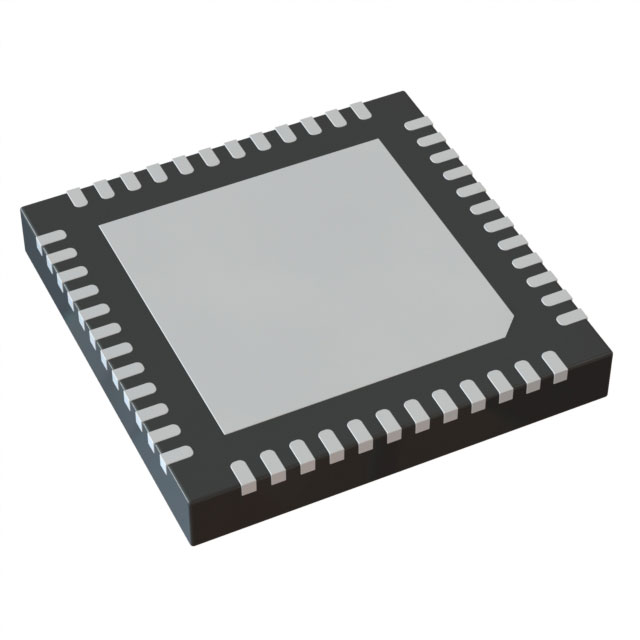
The MAX14866 is a 16-channel, high-voltage (HV), analog SPST switch primarily intended for HV multiplexing in ultrasound applications.The MAX14866 operates from one only low-voltage supply (+5V) and does not require dedicated HV supplies, resulting in cost-saving and system simplification. Moreover, for in-probe applications, HV supplies do not need to be associated with the MAX14866 in the probe/transducer head, resulting in greater safety and easier compliance with safety regulations.The MAX14866 features best-in-class performance in terms of bandwidth (up to 50MHz), charge injection (<100pC), and linear transmit input range (up to 210VPKPK). The low-signal switch RDSONis typically about 7Ω around 0V and remains flat in the entire input range ensuring extremely good linearity.The latchup-free SOI (Silicon-on-Insulator) technology and the wide analog range results in extremely high robustness during undershoots and overshoots that occur in ultrasound systems due to the resonant nature of the load.The status of the switches can be individually controlled through a high-speed SPI interface (up to 30MHz). Daisy-chain architecture is supported.Alternatively, switches can also be controlled with global control signal (SET and CLR) for bank selections or relay replacement applications.The MAX14866 is offered in two different packages: wafer-level packages (WLPs) and TQFNs. The 110-bump WLP size is only 5.53 x 5.47mm, resulting in less than 1.9mm2/channel footprint and allowing for very high levels of integration, which is especially beneficial for in-probe applications.The size of the TQFN package is an industry standard 48-pin, 7mm x 7mm package.ApplicationsMedical Ultrasound ImagingNDTPrintersRelays replacements
Technical Specifications
Parameters and characteristics for this part
| Specification | MAX14866UWZ+ |
|---|---|
| -3db Bandwidth | 80 MHz |
| Channel Capacitance (CD(off)) | 11 pF |
| Channel Capacitance (CS(off)) | 7.7 pF |
| Charge Injection | 100 pC |
| Crosstalk | -62 dB |
| Current - Leakage (Max) | 1 µA |
| Demultiplexer Outputs | 1 |
| Mounting Type | Surface Mount |
| Multiplexer Inputs | 1 |
| Number of Circuits | 16 |
| On-State Resistance (Max) | 13 Ohm |
| Operating Temperature (Max) | 85 °C |
| Operating Temperature (Min) | 0 °C |
| Package / Case | 110-WFBGA, WLBGA |
| Package Length | 5.5 mm |
| Package Name | 110-WLP |
| Package Width | 5.44 mm |
| Switch Circuit Type | SPST |
| Switch Contact | NO |
| Switch Time Toff (Max) | 4 µs |
| Switch Time Ton (Max) | 4 µs |
| Voltage - Supply, Single (V+) (Maximum) | 5.5 V |
| Voltage - Supply, Single (V+) (Minimum) | 1.7 V |
Pricing
Prices provided here are for design reference only. For realtime values and availability, please visit the distributors directly
Sign in to see pricing
Create a free account to access distributor pricing data.
CAD
3D models and CAD resources for this part
Documents
Technical documentation and resources