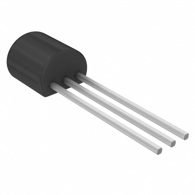
VN4012L-G
ActiveMOSFET, N-CHANNEL ENHANCEMENT-MODE, 400V, 12 OHM
Deep-Dive with AI
Search across all available documentation for this part.

VN4012L-G
ActiveMOSFET, N-CHANNEL ENHANCEMENT-MODE, 400V, 12 OHM
Deep-Dive with AI
Technical Specifications
Parameters and characteristics for this part
| Specification | VN4012L-G |
|---|---|
| Current - Continuous Drain (Id) @ 25°C | 160 mA |
| Drain to Source Voltage (Vdss) | 400 V |
| Drive Voltage (Max Rds On, Min Rds On) | 4.5 V |
| FET Type | N-Channel |
| Input Capacitance (Ciss) (Max) @ Vds | 110 pF |
| Mounting Type | Through Hole |
| Operating Temperature [Max] | 150 °C |
| Operating Temperature [Min] | -55 °C |
| Package / Case | TO-226-3, TO-92-3 |
| Power Dissipation (Max) | 1 W |
| Rds On (Max) @ Id, Vgs | 12 Ohm |
| Supplier Device Package | TO-92-3 |
| Technology | MOSFET (Metal Oxide) |
| Vgs (Max) | 20 V |
Pricing
Prices provided here are for design reference only. For realtime values and availability, please visit the distributors directly
| Distributor | Package | Quantity | $ | |
|---|---|---|---|---|
| Digikey | Bag | 1 | $ 2.00 | |
| 25 | $ 1.66 | |||
| 100 | $ 1.51 | |||
| Microchip Direct | BAG | 1 | $ 2.00 | |
| 25 | $ 1.66 | |||
| 100 | $ 1.51 | |||
| 1000 | $ 1.26 | |||
| 5000 | $ 1.15 | |||
| 10000 | $ 1.09 | |||
VN4012 Series
MOSFET, N-Channel Enhancement-Mode, 400V, 12 Ohm
| Part | Operating Temperature [Min] | Operating Temperature [Max] | Drain to Source Voltage (Vdss) | Package / Case | Technology | Rds On (Max) @ Id, Vgs | Current - Continuous Drain (Id) @ 25°C | Power Dissipation (Max) | FET Type | Vgs (Max) | Supplier Device Package | Drive Voltage (Max Rds On, Min Rds On) | Mounting Type | Input Capacitance (Ciss) (Max) @ Vds |
|---|---|---|---|---|---|---|---|---|---|---|---|---|---|---|
Microchip Technology VN4012L-G | -55 °C | 150 °C | 400 V | TO-226-3, TO-92-3 | MOSFET (Metal Oxide) | 12 Ohm | 160 mA | 1 W | N-Channel | 20 V | TO-92-3 | 4.5 V | Through Hole | 110 pF |
Description
General part information
VN4012 Series
This enhancement-mode (normally-off) transistor utilizes a vertical DMOS structure and well-proven, silicon-gate manufacturing process. This combination produces a device with the power handling capabilities of bipolar transistors and the high input impedance and positive temperature coefficient inherent in MOS devices. Characteristic of all MOS structures, this device is free from thermal runaway and thermally-induced secondary breakdown.
Vertical DMOS FETs are ideally suited to a wide range of switching and amplifying applications where very low threshold voltage, high breakdown voltage, high input impedance, low input capacitance, and fast switching speeds are desired.
Documents
Technical documentation and resources


