Technical Specifications
Parameters and characteristics for this part
| Specification | STHV200Q |
|---|---|
| Mounting Type | Surface Mount |
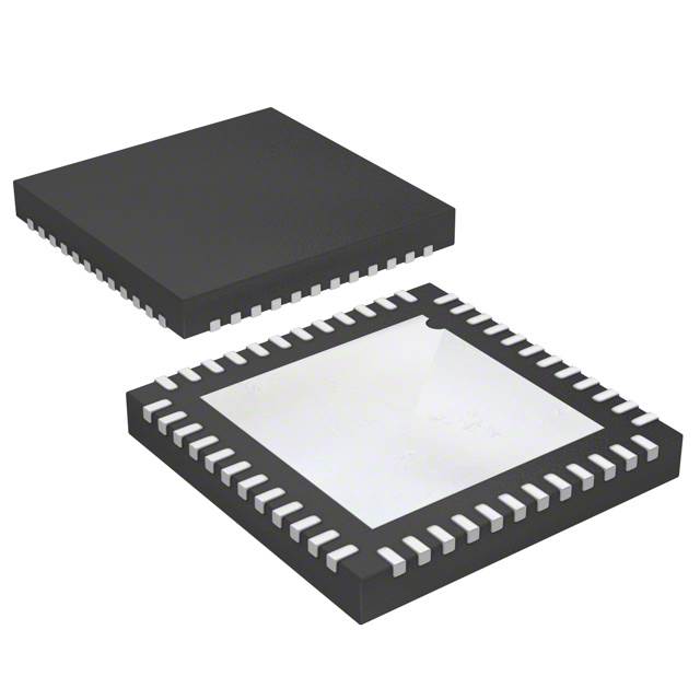
| Package / Case | 48-VFQFN Exposed Pad |
| Supplier Device Package | 48-QFN (7x7) |
| Type | Driver |
Pricing
Prices provided here are for design reference only. For realtime values and availability, please visit the distributors directly
| Distributor | Package | Quantity | $ | |
|---|---|---|---|---|
| Digikey | Bulk | 1560 | $ 28.14 | |
Description
General part information
STHV200Q Series
The STHV200 is a fully integrated high-voltage driver including both a dual-channel linear and a dual-channel pulser driver. Pulser and linear share the same high-voltage output node XDCR and allow the user to select which output stage to use according to each specific application. This solution allows to optimize the final performances in terms of flexibility, harmonic contents, and power consumption, meeting the most demanding needs for the end application. The device can support a wide range of operating modes as pulsed wave (PW), continuous wave (CW), and elastography.
Each linear driver is a non-inverting configuration operational amplifier (op-amp) with four programmable gains (39 dB, 36 dB, 32.5 dB, and 24 dB) providing in this way the best performances for the output signal in a range between 1 Vpp and 180 Vpp. Linear drivers have been designed to optimize harmonic and noise performances thanks to a bandwidth up to 20 MHz when the maximum gain is set. Bandwidth increases reducing the gain and it reaches 25 MHz with the minimum gain setting. Each op-amp drives directly the corresponding XDCR output node without any diode connections, generating a very clean output signal and minimizing odd distortion. An internal circuit fully isolates the output to its parasitic capacitances during pulser driver activity. Fast turn-on and off times of 1.8 us and 0.6 us make the device suitable also for near-field images. A new and dedicated structure, named "active diodes", mitigates the glitch injection during the linear turn-on/off.
Pulser drivers are designed in a half-bridge configuration with a programmable saturation current (0.5 A, 1 A, 1.5 A, and 2 A) for both high-side and low-side. The generated output voltage can vary from 2 Vpp up to 200 Vpp. A real-to-zero Clamp structure with a current capability of 1 A can directly force the output node to ground. Users can fine-tune the delays of both positive and negative edges and also choose a dedicated setting for CW and elastography mode, thus optimizing the performances and the power consumption in each operative condition.
Documents
Technical documentation and resources