


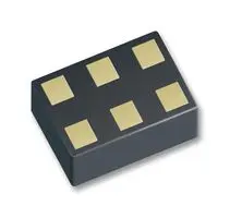

Description
General part information
BGS12P2 Series
The BGS12P2L6 is a general purpose high power SPDT switch, designed to cover a broad range applications from 0.05 to 6 GHz and therefore excellent for 5G sub-6 GHz. Its outstanding RF performance optimizes the transmitting path (TRx) of LTE/5G mobile phones. The chip integrates on-chip CMOS logic driven by a simple, single-pin CMOS or TTL compatible control input signal. Unlike GaAs technology, external DC blocking capacitors at the RF ports are only required if DC voltage is applied externally. The BGS12P2L6 RF switch is manufactured in Infineon’s patented MOS technology, offering the performance of GaAs with the economy and integration of conventional CMOS including the inherent higher ESD robustness. The device has a very small size of only 0.7 x 1.1 mm2 and a maximum height of 0.31 mm.
Technical Specifications
Parameters and characteristics for this part
| Specification | BGS12P2L6E6327XTSA1 |
|---|---|
| Circuit | SPDT |
| Frequency Range (Max) | 6 GHz |
| Frequency Range (Min) | 50 MHz |
| IIP3 | 74 dBm |
| Impedance | 50 Ohm |
| Insertion Loss | 0.51 dB |
| Isolation | 27 dB |
| Mounting Type | Surface Mount |
| Operating Temperature (Max) | 85 °C |
| Operating Temperature (Min) | -40 °C |
| Package / Case | 6-XFDFN |
| Package Name | PG-TSLP-6-4 |
| RF Type | GSM, W-CDMA, LTE |
| Test Frequency | 5.925 GHz |
| Voltage - Supply (Maximum) | 3.4 V |
| Voltage - Supply (Minimum) | 1.65 V |
Pricing
Prices provided here are for design reference only. For realtime values and availability, please visit the distributors directly
Sign in to see pricing
Create a free account to access distributor pricing data.
CAD
3D models and CAD resources for this part
Documents
Technical documentation and resources