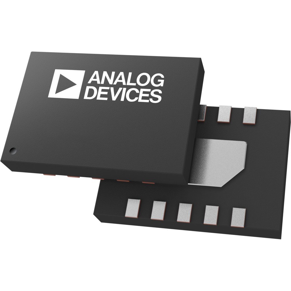
MAX5805BATB+
UnknownULTRA-SMALL, SINGLE-CHANNEL, 8-/10-/12-BIT BUFFERED OUTPUT VOLTAGE DACS WITH INTERNAL REFERENCE AND I2C INTERFACE
MAX5805BATB+
UnknownULTRA-SMALL, SINGLE-CHANNEL, 8-/10-/12-BIT BUFFERED OUTPUT VOLTAGE DACS WITH INTERNAL REFERENCE AND I2C INTERFACE
Description
General part information
MAX5805 Series
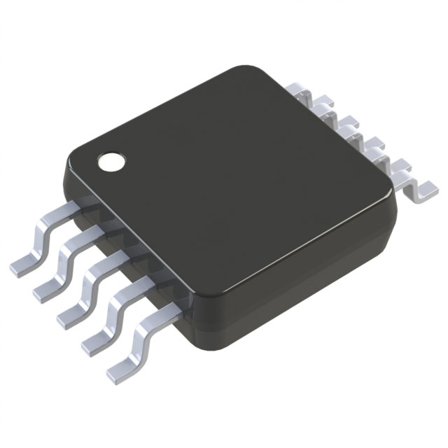
The MAX5803/MAX5804/MAX5805 single-channel, low-power, 8-/10-/12-bit, voltage-output digital-to-analog converters (DACs) include output buffers and an internal reference that is selectable to be 2.048V, 2.500V, or 4.096V. The MAX5803/MAX5804/MAX5805 accept a wide supply voltage range of 2.7V to 5.5V with extremely low power (< 1mW) consumption to accommodate most low-voltage applications. A precision external reference input allows rail-to-rail operation and presents a 100kΩ (typ) load to an external reference.The MAX5803/MAX5804/MAX5805 have an I2C-compatible, 2-wire interface that operates at clock rates up to 400kHz. The DAC output is buffered and has a low supply current of 155µA (typical at 3V) and a low offset error of ±0.5mV (typical). On power-up, the MAX5803/MAX5804/MAX5805 reset the DAC outputs to zero, providing additional safety for applications that drive valves or other transducers which need to be off on power-up. The internal reference is initially powered down to allow use of an external reference.The MAX5803/MAX5804/MAX5805 include a user-configurable active-low asynchronous input, active-low AUX for additional flexibility. This input can be programmed to asynchronously clear (active-low CLR) or temporarily gate (active-low GATE) the DAC output to a user-programmable value. A dedicated active-low asynchronous LDAC input is also included. This allows simultaneous output updates of multiple devices.The MAX5803/MAX5804/MAX5805 are available in 10-pin TDFN/µMAX®packages and are specified over the -40°C to +125°C temperature range.ApplicationsAutomatic Tuning and Optical ControlData AcquisitionGain and Offset AdjustmentPortable InstrumentationPower Amplifier Control and BiasingProcess Control and Servo LoopsProgrammable Voltage and Current Sources
Technical Specifications
Parameters and characteristics for this part
| Specification | MAX5805BATB+ |
|---|---|
| Architecture | R-2R |
| Data Interface | I2C |
| Differential Output | No |
| DNL (LSB) Tolerance | 0.2 LSB |
| INL (LSB) Tolerance | 0.5 LSB |
| Mounting Type | Surface Mount |
| Number of Bits | 12 bits |
| Number of D/A Converters | 1 count |
| Operating Temperature (Max) | 125 °C |
| Operating Temperature (Min) | -40 °C |
| Output Type | Voltage - Buffered |
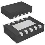
| Package / Case | 10-WFDFN Exposed Pad |
| Package Length | 3 mm |
| Package Name | 10-TDFN |
| Package Width | 2 mm |
| Reference Type | External, Internal |
| Settling Time (Typical) | 6.3 µs |
| Voltage - Supply, Analog (Max) | 5.5 V |
| Voltage - Supply, Analog (Min) | 2.7 V |
| Voltage - Supply, Digital (Max) | 5.5 V |
| Voltage - Supply, Digital (Min) | 2.7 V |
Pricing
Prices provided here are for design reference only. For realtime values and availability, please visit the distributors directly
Sign in to see pricing
Create a free account to access distributor pricing data.
CAD
3D models and CAD resources for this part
Documents
Technical documentation and resources