


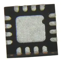
AD5697RBCPZ-RL7
ActiveDUAL 12-BITNANODAC+™ WITH 2PPM/°C REFERENCE, I2C INTERFACE
AD5697RBCPZ-RL7
ActiveDUAL 12-BITNANODAC+™ WITH 2PPM/°C REFERENCE, I2C INTERFACE
Description
General part information
AD5697R Series
The AD5697R, a member of thenanoDAC+™ family, is a low power, dual, 12-bit buffered voltage output digital-to-analog converter (DAC). The device includes a 2.5 V, 2 ppm/°C internal reference (enabled by default) and a gain select pin giving a full-scale output of 2.5 V (gain = 1) or 5 V (gain = 2). The AD5697R operates from a single 2.7 V to 5.5 V supply, is guaranteed monotonic by design, and exhibits less than 0.1% FSR gain error and 1.5 mV offset error performance. The device is available in a 3 mm × 3 mm LFCSP and a TSSOP package.The AD5697R also incorporates a power-on reset circuit and a RSTSEL pin that ensure that the DAC outputs power up to zero scale or midscale and remain there until a valid write takes place. It contains a per channel power-down feature that reduces the current consumption of the device to 4 µA at 3 V while in power-down mode.The AD5697R uses a versatile 2-wire serial interface that operates at clock rates up to 400 kHz and includes a VLOGICpin intended for 1.8 V/3 V/5 V logic.PRODUCT HIGHLIGHTSPrecision DC Performance.TUE: ±0.1% of FSR maximumOffset error: ±1.5 mV maximumGain error: ±0.1% of FSR maximumLow Drift 2.5 V On-Chip Reference.2 ppm/°C typical temperature coefficient5 ppm/°C maximum temperature coefficientTwo Package Options.3 mm × 3 mm, 16-lead LFCSP16-lead TSSOPAPPLICATIONSBase station power amplifiersProcess controls (programmable logic controller [PLC] I/O cards)Industrial automationData acquisition systems
Technical Specifications
Parameters and characteristics for this part
| Specification | AD5697RBCPZ-RL7 |
|---|---|
| Architecture | String DAC |
| Data Interface | I2C |
| Differential Output | No |
| DNL (LSB) Tolerance | 1 LSB, 1 LSB |
| INL (LSB) Tolerance | 0.12 LSB |
| INL (Max) (LSB) | 0.12 LSB |
| Mounting Type | Surface Mount |
| Number of Bits | 12 bits |
| Number of D/A Converters | 2 count |
| Operating Temperature (Max) | 105 °C |
| Operating Temperature (Min) | -40 °C |
| Output Type | Voltage - Buffered |
| Package / Case | 16-WFQFN Exposed Pad, CSP |
| Package Length | 3 mm |
| Package Name | 16-LFCSP |
| Package Width | 3 mm |
| Reference Type | External, Internal |
| Settling Time | 7 µs |
| Voltage - Supply, Analog (Max) | 5.5 V |
| Voltage - Supply, Analog (Min) | 2.7 V |
| Voltage - Supply, Digital (Max) | 5.5 V |
| Voltage - Supply, Digital (Min) | 1.8 V |
Pricing
Prices provided here are for design reference only. For realtime values and availability, please visit the distributors directly
Sign in to see pricing
Create a free account to access distributor pricing data.
CAD
3D models and CAD resources for this part
Documents
Technical documentation and resources

