HMC850LC3
Active28 GBPS 1:2 FANOUT BUFFER WITH PROGRAMMABLE OUTPUT VOLTAGE
HMC850LC3
Active28 GBPS 1:2 FANOUT BUFFER WITH PROGRAMMABLE OUTPUT VOLTAGE
Description
General part information
HMC850 Series
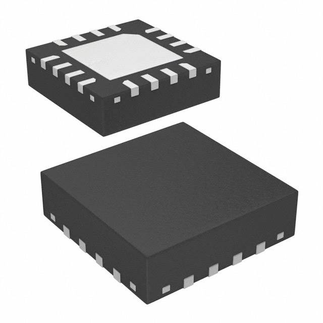
The HMC850LC3 is a 1:2 Fanout Buffer designed to support data transmission rates up to 28 Gbps, and clock frequencies as high as 20 GHz. All differential inputs and outputs are DC coupled and terminated on chip with 50 Ω resistors to the positive supply, ground. The outputs may be used in either single-ended or differential modes, and should be AC or DC coupled into 50 Ω resistors connected to ground.The HMC850LC3 also features an output level control pin, VR which allows for loss compensation or for signal level optimization. The HMC850LC3 operates from a single -3.3V DC supply and is available in a ceramic RoHS compliant 3×3 mm SMT package.APPLICATIONSRF ATE ApplicationsBroadband Test & MeasurementSerial Data Transmission up to 28 GbpsClock Buffering up to 20 GHz
Technical Specifications
Parameters and characteristics for this part
| Specification | HMC850LC3 |
|---|---|
| Differential Input | Yes |
| Differential Output | Yes |
| Frequency - Max | 20 Gbps |
| Input | CML |
| Input Ratio | 1 |
| Mounting Type | Surface Mount |
| Number of Circuits | 1 |
| Operating Temperature (Max) | 85 °C |
| Operating Temperature (Min) | -40 °C |
| Output | CML |
| Output Ratio | 2 |
| Package / Case | 16-VFCQFN Exposed Pad |
| Package Length | 3 mm |
| Package Name | 16-CSMT |
| Package Width | 3 mm |
| Type | Fanout Buffer (Distribution) |
| Voltage - Supply (Maximum) | -3 V |
| Voltage - Supply (Minimum) | -3.6 V |
Pricing
Prices provided here are for design reference only. For realtime values and availability, please visit the distributors directly
Sign in to see pricing
Create a free account to access distributor pricing data.
CAD
3D models and CAD resources for this part
Documents
Technical documentation and resources