


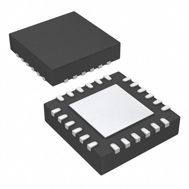
BD9P108MUF-CE2
ActiveRohm Semiconductor
NANO PULSE CONTROL™ 3.5V TO 40V INPUT, 1A SINGLE 2.2MHZ BUCK DC/DC CONVERTER FOR AUTOMOTIVE

BD9P108MUF-CE2
ActiveRohm Semiconductor
NANO PULSE CONTROL™ 3.5V TO 40V INPUT, 1A SINGLE 2.2MHZ BUCK DC/DC CONVERTER FOR AUTOMOTIVE
Description
General part information
BD9P108MUF-C Series
BD9P108MUF-C is current mode synchronous buck DC/DC converter integrating POWER MOSFETs.
Technical Specifications
Parameters and characteristics for this part
| Specification | BD9P108MUF-CE2 |
|---|---|
| Current - Output | 1 A |
| Frequency - Switching | 2.2 MHz |
| Function | Step-Down |
| Grade | Automotive |
| Mounting Type | Surface Mount |
| Number of Outputs | 1 |
| Operating Temperature (Max) | 125 °C |
| Operating Temperature (Min) | -40 °C |
| Output Configuration | Positive |
| Output Type | Adjustable |
| Package / Case | 24-VFQFN Exposed Pad |
| Package Name | VQFN24FV4040 |
| Qualification | AEC-Q100 |
| Synchronous Rectifier | Yes |
| Topology | Buck |
| Voltage - Input (Max) | 40 V |
| Voltage - Input (Min) | 3.5 V |
| Voltage - Output (Max) | 8.5 V |
| Voltage - Output (Min/Fixed) | 0.8 V |
Pricing
Prices provided here are for design reference only. For realtime values and availability, please visit the distributors directly
Sign in to see pricing
Create a free account to access distributor pricing data.
CAD
3D models and CAD resources for this part
Documents
Technical documentation and resources
Datasheet
Basics of Thermal Resistance and Heat Dissipation
θ<sub>JA</sub> and Ψ<sub>JT</sub>
Method for Determining Constants of Peripheral Parts of Buck DC/DC Converter
Thermal Resistance
What Is Thermal Design
Bootstrap Circuit in the Buck Converter
VQFN24FV4040 Package Information
Considering Polarity of Power Inductor to Reduce Radiated Emission of DC-DC converter
Cutting-Edge Web Simulation Tool "ROHM Solution Simulator" Capable of Complete Circuit Verification of Power Devices and Driver ICs
Capacitor Calculation for Buck converter IC
Three Steps for Successful Design of DC-DC Converters
Overview of ROHM's Simulation Models(for ICs and Discrete Semiconductors)
The Important Points of Multi-layer Ceramic Capacitor Used in Buck Converter circuit
Heat Dissipation Effect of Thermal Via in Exposed Pad Type Package
Evaluation Board User's Guide for BD9P108MUF-TSB-001
PCB Layout Essential Check sheet for Switching Regulator
Power Supply Sequence Circuit with General Purpose Power Supply IC
Two-Resistor Model for Thermal Simulation
Calculation of Power Dissipation in Switching Circuit
Types of Capacitors Used for Output Smoothing of Switching Regulators and their Precautions
Simulation Guide for BD9P108MUF-C / Frequency Response (ROHM Solution Simulator)
Judgment Criteria of Thermal Evaluation
How to Use the Thermal Resistance and Thermal Characteristics Parameters
Calculation of Power Loss (Synchronous)
Measurement Method for Phase Margin with Frequency Response Analyzer (FRA)
Precautions for PCB Layout Regarding Common Mode Filters
Impedance Characteristics of Bypass Capacitor
Diode Selection Method for Asynchronous Converter
Five Steps for Successful Thermal Design of IC
Suppression Method of Switching Noise Using Linear Regulator and Low Pass Filter
Phase Compensation Design for Current Mode Buck Converter
Considering Input Filter to Reduce Conducted Emissions by DCDC Converter
PCB Layout Techniques of Buck Converter
Factory Information
Design Guide and Example of Stencil for Exposed Pad
How to Use the Two-Resistor Model
BD9P108MUF-C SPICE Modeling Report
Considerations for Power Inductors Used for Buck Converters
Snubber Circuit for Buck Converter IC
Solder Joint Rate and Thermal Resistance of Exposed Pad
θ<sub>JC</sub> and Ψ<sub>JT</sub>
Efficiency of Buck Converter
Precautions When Measuring the Rear of the Package with a Thermocouple
Step-down DC-DC converter PCB layout EMC Design guide
Inductor Calculation for Buck converter IC
Resistor Value Table to set Output Voltage of Buck Converter IC
PCB Layout Thermal Design Guide
Method for Calculating Junction Temperature from Transient Thermal Resistance Data
Technical Data Sheet EN