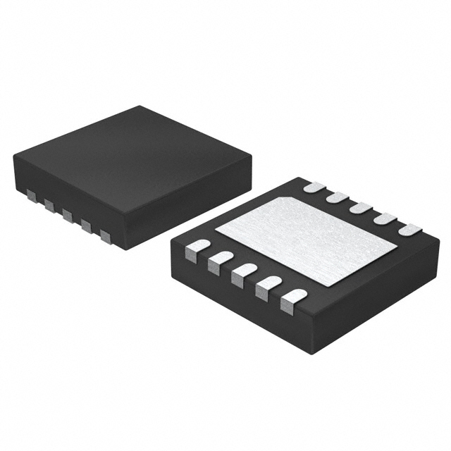
AD7687BCPZ-R2
Active16-BIT, 1.5 LSB INL, 250 KSPS PULSAR™ DIFFERENTIAL ADC IN MSOP/QFN
Deep-Dive with AI
Search across all available documentation for this part.
AD7687BCPZ-R2
Active16-BIT, 1.5 LSB INL, 250 KSPS PULSAR™ DIFFERENTIAL ADC IN MSOP/QFN
Deep-Dive with AI
Technical Specifications
Parameters and characteristics commom to parts in this series
| Specification | AD7687BCPZ-R2 | AD7687 Series |
|---|---|---|
| Architecture | - | SAR |
| Configuration | - | S/H-ADC |
| Data Interface | - | SPI, DSP |
| Input Type | - | Differential |
| Mounting Type | Surface Mount | Surface Mount |
| Number of A/D Converters | - | 1 |
| Number of Bits | - | 16 bits |
| Number of Inputs | - | 1 |
| Operating Temperature | - | -40 °C |
| Operating Temperature | - | 85 °C |
| Package / Case | 10-VFDFN Exposed Pad, CSP | 10-VFDFN Exposed Pad, CSP, 10-TFSOP, 10-MSOP |
| Ratio - S/H:ADC | - | 1:1 |
| Reference Type | - | External |
| Sampling Rate (Per Second) | - | 250 k |
| Supplier Device Package | 10-LFCSP-WD (3x3) | 10-LFCSP-WD (3x3), 10-MSOP |
| Voltage - Supply, Analog | - | 5.5 V |
| Voltage - Supply, Analog | - | 2.3 V |
| Voltage - Supply, Digital | - | 2.3 V |
| Voltage - Supply, Digital | - | 5.5 V |
Pricing
Prices provided here are for design reference only. For realtime values and availability, please visit the distributors directly
AD7687 Series
16-Bit, 1.5 LSB INL, 250 kSPS PulSAR™Differential ADC in MSOP/QFN
| Part | Package / Case | Mounting Type | Supplier Device Package | Data Interface | Configuration | Voltage - Supply, Digital [Min] | Voltage - Supply, Digital [Max] | Voltage - Supply, Analog [Max] | Voltage - Supply, Analog [Min] | Input Type | Reference Type | Operating Temperature [Min] | Operating Temperature [Max] | Number of Bits | Architecture | Number of Inputs | Ratio - S/H:ADC | Number of A/D Converters | Sampling Rate (Per Second) |
|---|---|---|---|---|---|---|---|---|---|---|---|---|---|---|---|---|---|---|---|
10-VFDFN Exposed Pad, CSP | Surface Mount | 10-LFCSP-WD (3x3) | |||||||||||||||||
Analog Devices Inc AD7687BCPZRL7The AD76871 is a 16-bit, charge redistribution, successive approximation, analog-to-digital converter (ADC) that operates from a single power supply, VDD, between 2.3 V to 5.5 V. It contains a low power, high speed, 16-bit sampling ADC with no missing codes, an internal conversion clock, and a versatile serial interface port. The device also contains a low noise, wide bandwidth, short aperture delay track-and-hold circuit. On the CNV rising edge, the AD7687 the samples the voltage difference between IN+ and IN− pins, which can range from −VREFto +VREF. The reference voltage, VREF, is applied externally and can be set up to the supply voltage.The power consumption of the device scales linearly with throughput.The SPI-compatible serial interface also features the ability to daisy-chain several ADCs on a single 3-wire bus and provides an optional BUSY indicator by means of the SDI pin. It is compatible with 1.8 V, 2.5 V, 3 V, or 5 V logic using the separate supply VIO.The AD7687 comes in a 10-lead MSOP or a 10-lead LFCSP with operation specified from −40°C to +85°C.APPLICATIONSBattery-powered equipmentData acquisitionsInstrumentationMedical instrumentsProcess controls | 10-VFDFN Exposed Pad, CSP | Surface Mount | 10-LFCSP-WD (3x3) | DSP, SPI | S/H-ADC | 2.3 V | 5.5 V | 5.5 V | 2.3 V | Differential | External | -40 °C | 85 °C | 16 bits | SAR | 1 | 1:1 | 1 | 250 k |
Analog Devices Inc AD7687BRMZRL7The AD76871 is a 16-bit, charge redistribution, successive approximation, analog-to-digital converter (ADC) that operates from a single power supply, VDD, between 2.3 V to 5.5 V. It contains a low power, high speed, 16-bit sampling ADC with no missing codes, an internal conversion clock, and a versatile serial interface port. The device also contains a low noise, wide bandwidth, short aperture delay track-and-hold circuit. On the CNV rising edge, the AD7687 the samples the voltage difference between IN+ and IN− pins, which can range from −VREFto +VREF. The reference voltage, VREF, is applied externally and can be set up to the supply voltage.The power consumption of the device scales linearly with throughput.The SPI-compatible serial interface also features the ability to daisy-chain several ADCs on a single 3-wire bus and provides an optional BUSY indicator by means of the SDI pin. It is compatible with 1.8 V, 2.5 V, 3 V, or 5 V logic using the separate supply VIO.The AD7687 comes in a 10-lead MSOP or a 10-lead LFCSP with operation specified from −40°C to +85°C.APPLICATIONSBattery-powered equipmentData acquisitionsInstrumentationMedical instrumentsProcess controls | 10-MSOP, 10-TFSOP | Surface Mount | 10-MSOP | DSP, SPI | S/H-ADC | 2.3 V | 5.5 V | 5.5 V | 2.3 V | Differential | External | -40 °C | 85 °C | 16 bits | SAR | 1 | 1:1 | 1 | 250 k |
10-VFDFN Exposed Pad, CSP | Surface Mount | 10-LFCSP-WD (3x3) | DSP, SPI | S/H-ADC | 2.3 V | 5.5 V | 5.5 V | 2.3 V | Differential | External | -40 °C | 85 °C | 16 bits | SAR | 1 | 1:1 | 1 | 250 k | |
Analog Devices Inc AD7687BRMZThe AD76871 is a 16-bit, charge redistribution, successive approximation, analog-to-digital converter (ADC) that operates from a single power supply, VDD, between 2.3 V to 5.5 V. It contains a low power, high speed, 16-bit sampling ADC with no missing codes, an internal conversion clock, and a versatile serial interface port. The device also contains a low noise, wide bandwidth, short aperture delay track-and-hold circuit. On the CNV rising edge, the AD7687 the samples the voltage difference between IN+ and IN− pins, which can range from −VREFto +VREF. The reference voltage, VREF, is applied externally and can be set up to the supply voltage.The power consumption of the device scales linearly with throughput.The SPI-compatible serial interface also features the ability to daisy-chain several ADCs on a single 3-wire bus and provides an optional BUSY indicator by means of the SDI pin. It is compatible with 1.8 V, 2.5 V, 3 V, or 5 V logic using the separate supply VIO.The AD7687 comes in a 10-lead MSOP or a 10-lead LFCSP with operation specified from −40°C to +85°C.APPLICATIONSBattery-powered equipmentData acquisitionsInstrumentationMedical instrumentsProcess controls | 10-MSOP, 10-TFSOP | Surface Mount | 10-MSOP | DSP, SPI | S/H-ADC | 2.3 V | 5.5 V | 5.5 V | 2.3 V | Differential | External | -40 °C | 85 °C | 16 bits | SAR | 1 | 1:1 | 1 | 250 k |
Description
General part information
AD7687 Series
The AD76871 is a 16-bit, charge redistribution, successive approximation, analog-to-digital converter (ADC) that operates from a single power supply, VDD, between 2.3 V to 5.5 V. It contains a low power, high speed, 16-bit sampling ADC with no missing codes, an internal conversion clock, and a versatile serial interface port. The device also contains a low noise, wide bandwidth, short aperture delay track-and-hold circuit. On the CNV rising edge, the AD7687 the samples the voltage difference between IN+ and IN− pins, which can range from −VREFto +VREF. The reference voltage, VREF, is applied externally and can be set up to the supply voltage.The power consumption of the device scales linearly with throughput.The SPI-compatible serial interface also features the ability to daisy-chain several ADCs on a single 3-wire bus and provides an optional BUSY indicator by means of the SDI pin. It is compatible with 1.8 V, 2.5 V, 3 V, or 5 V logic using the separate supply VIO.The AD7687 comes in a 10-lead MSOP or a 10-lead LFCSP with operation specified from −40°C to +85°C.APPLICATIONSBattery-powered equipmentData acquisitionsInstrumentationMedical instrumentsProcess controls
Documents
Technical documentation and resources