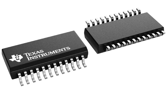
CDC5801ADBQ
ActiveLOW-JITTER CLOCK MULTIPLIER & DIVIDER WITH PROGRAMMABLE DELAY & PHASE ALIGNMENT
Deep-Dive with AI
Search across all available documentation for this part.

CDC5801ADBQ
ActiveLOW-JITTER CLOCK MULTIPLIER & DIVIDER WITH PROGRAMMABLE DELAY & PHASE ALIGNMENT
Deep-Dive with AI
Technical Specifications
Parameters and characteristics commom to parts in this series
| Specification | CDC5801ADBQ | CDC5801A Series |
|---|---|---|
| Differential - Input:Output | No/Yes | No/Yes |
| Frequency - Max [Max] | 500 MHz | 500 MHz |
| Input | LVCMOS, LVTTL | LVCMOS, LVTTL |
| Mounting Type | Surface Mount | Surface Mount |
| Number of Circuits | 1 | 1 |
| Operating Temperature [Max] | 85 °C | 85 °C |
| Operating Temperature [Min] | -40 °C | -40 °C |
| Output | LVPECL, LVTTL, LVDS | LVPECL, LVTTL, LVDS |
| Package / Case | 24-SSOP | 24-SSOP |
| PLL | Yes with Bypass | Yes with Bypass |
| Ratio - Input:Output [custom] | 1:1 | 1:1 |
| Supplier Device Package | 24-SSOP | 24-SSOP |
| Type | PLL Multiplier/Divider | PLL Multiplier/Divider |
| Voltage - Supply [Max] | 3.6 V | 3.6 V |
| Voltage - Supply [Min] | 3 V | 3 V |
Pricing
Prices provided here are for design reference only. For realtime values and availability, please visit the distributors directly
| Distributor | Package | Quantity | $ | |
|---|---|---|---|---|
| Digikey | Tube | 150 | $ 7.61 | |
| Texas Instruments | TUBE | 1 | $ 7.79 | |
| 100 | $ 6.35 | |||
| 250 | $ 4.99 | |||
| 1000 | $ 4.23 | |||
CDC5801A Series
Low-jitter clock multiplier & divider with programmable delay & phase alignment
| Part | Differential - Input:Output | Voltage - Supply [Max] | Voltage - Supply [Min] | Package / Case | Ratio - Input:Output [custom] | Type | Input | PLL | Frequency - Max [Max] | Operating Temperature [Min] | Operating Temperature [Max] | Number of Circuits | Output | Supplier Device Package | Mounting Type |
|---|---|---|---|---|---|---|---|---|---|---|---|---|---|---|---|
Texas Instruments CDC5801ADBQR | No/Yes | 3.6 V | 3 V | 24-SSOP | 1:1 | PLL Multiplier/Divider | LVCMOS, LVTTL | Yes with Bypass | 500 MHz | -40 °C | 85 °C | 1 | LVDS, LVPECL, LVTTL | 24-SSOP | Surface Mount |
Texas Instruments CDC5801ADBQ | No/Yes | 3.6 V | 3 V | 24-SSOP | 1:1 | PLL Multiplier/Divider | LVCMOS, LVTTL | Yes with Bypass | 500 MHz | -40 °C | 85 °C | 1 | LVDS, LVPECL, LVTTL | 24-SSOP | Surface Mount |
Description
General part information
CDC5801A Series
The CDC5801A device provides clock multiplication and division from a single-ended reference clock (REFCLK) to a differential output pair (CLKOUT/CLKOUTB). The multiply and divide terminals (MULT/DIV0:1) provide selection for frequency multiplication and division ratios, generating CLKOUT/CLOUTKB frequencies ranging from 12.5 MHz to 500 MHz with a clock input reference (REFCLK) ranging from 19 MHz to 125 MHz.
The implemented phase aligner provides the possibility to phase align (zero delay) between CLKOUT/CLKOUTB and REFCLK or any other CLK in the system by feeding the clocks that need to be aligned to the DLYCTRL and the LEADLAG terminals.
The phase aligner also allows the user to delay or advance the CLKOUT/CLKOUTB with steps of 2.6 mUI (unit interval). For every rising edge on the DLYCTRL terminal, the output clocks are delayed by 2.6-mUI step size as long as there is low on the LEADLAG terminal. Similarly, for every rising edge on the DLYCTRL terminal, the output clocks are advanced by 2.6-mUI step size as long as there is high on the LEADLAG terminal. The CDC5801A has a fail-safe power up initialization state-machine which supports proper operation under all power up conditions. As the phase between REFCLK and CLKOUT/CLKOUTB is random after power up, the application may implement a self calibration routine at power up to produce a certain phase start position, before programming a fixed delay with the clock on the DLYCTRL terminal.
Documents
Technical documentation and resources


