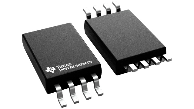
CDCS503TPWRQ1
ActiveAUTOMOTIVE CLOCK BUFFER/CLOCK MULTIPLIER WITH OPTIONAL SSC
Deep-Dive with AI
Search across all available documentation for this part.

CDCS503TPWRQ1
ActiveAUTOMOTIVE CLOCK BUFFER/CLOCK MULTIPLIER WITH OPTIONAL SSC
Technical Specifications
Parameters and characteristics for this part
| Specification | CDCS503TPWRQ1 |
|---|---|
| Differential - Input:Output [custom] | False |
| Differential - Input:Output [custom] | False |
| Frequency - Max [Max] | 108 MHz |
| Grade | Automotive |
| Input | LVCMOS |
| Mounting Type | Surface Mount |
| Number of Circuits | 1 |
| Operating Temperature [Max] | 105 ░C |
| Operating Temperature [Min] | -40 °C |
| Output | LVCMOS |
| Package / Case | 8-TSSOP (0.173", 4.40mm Width) |
| Qualification | AEC-Q100 |
| Ratio - Input:Output [custom] | 1:1 |
| Supplier Device Package | 8-TSSOP |
| Voltage - Supply [Max] | 3.6 V |
| Voltage - Supply [Min] | 3 V |
Pricing
Prices provided here are for design reference only. For realtime values and availability, please visit the distributors directly
| Distributor | Package | Quantity | $ | |
|---|---|---|---|---|
| Digikey | Cut Tape (CT) | 1 | $ 1.60 | |
| 10 | $ 1.44 | |||
| 25 | $ 1.36 | |||
| 100 | $ 1.16 | |||
| 250 | $ 1.08 | |||
| 500 | $ 0.95 | |||
| 1000 | $ 0.79 | |||
| Digi-Reel® | 1 | $ 1.60 | ||
| 10 | $ 1.44 | |||
| 25 | $ 1.36 | |||
| 100 | $ 1.16 | |||
| 250 | $ 1.08 | |||
| 500 | $ 0.95 | |||
| 1000 | $ 0.79 | |||
| Tape & Reel (TR) | 2000 | $ 0.73 | ||
| 6000 | $ 0.71 | |||
| 10000 | $ 0.68 | |||
| Texas Instruments | LARGE T&R | 1 | $ 1.20 | |
| 100 | $ 0.99 | |||
| 250 | $ 0.71 | |||
| 1000 | $ 0.54 | |||
CDCS503-Q1 Series
Automotive clock buffer/clock multiplier with optional SSC
| Part | Supplier Device Package | Ratio - Input:Output [custom] | Voltage - Supply [Max] | Voltage - Supply [Min] | Input | Differential - Input:Output [custom] | Differential - Input:Output [custom] | Qualification | Mounting Type | Grade | Output | Operating Temperature [Min] | Operating Temperature [Max] | Package / Case | Frequency - Max [Max] | Number of Circuits |
|---|---|---|---|---|---|---|---|---|---|---|---|---|---|---|---|---|
Texas Instruments CDCS503TPWRQ1 | 8-TSSOP | 1:1 | 3.6 V | 3 V | LVCMOS | AEC-Q100 | Surface Mount | Automotive | LVCMOS | -40 °C | 105 ░C | 8-TSSOP (0.173", 4.40mm Width) | 108 MHz | 1 |
Description
General part information
CDCS503-Q1 Series
The CDCS503-Q1 device is a spread spectrum capable, LVCMOS input clock buffer with selectable frequency multiplication.
It shares major functionality with the CDCS502 but uses a LVCMOS input stage instead of the crystal input stage of the CDCS502, and the CDCS503-Q1 has an output enable pin.
The device accepts a 3.3-V LVCMOS signal at the input.
Documents
Technical documentation and resources


