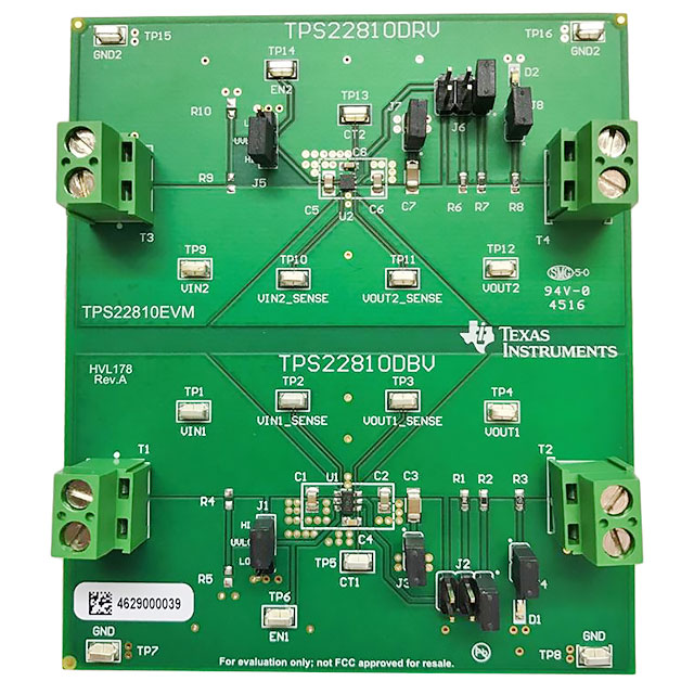
TPS22810EVM
ActiveEVALUATION MODULE
Deep-Dive with AI
Search across all available documentation for this part.
TPS22810EVM
ActiveEVALUATION MODULE
Deep-Dive with AI
Technical Specifications
Parameters and characteristics commom to parts in this series
| Specification | TPS22810EVM | TPS22810 Series |
|---|---|---|
| Contents | Board(s) | Board(s) |
| Current - Output (Max) | - | 2 - 3 A |
| Fault Protection | - | Over Temperature, UVLO |
| Features | - | Slew Rate Controlled, Load Discharge |
| Function | Power Distribution Switch (Load Switch) | Power Distribution Switch (Load Switch) |
| Grade | - | Automotive |
| Input Type | - | Non-Inverting |
| Interface | - | On/Off |
| Mounting Type | - | Surface Mount |
| Number of Outputs | - | 1 |
| Operating Temperature | - | 105 °C |
| Operating Temperature | - | -40 °C |
| Output Configuration | - | High Side |
| Output Type | - | N-Channel |
| Package / Case | - | SOT-23-6 |
| Primary Attributes | 1-Channel (Single) | 1-Channel (Single) |
| Qualification | - | AEC-Q100 |
| Ratio - Input:Output | - | 1:1 |
| Rds On (Typ) | - | 79 mOhm |
| Supplied Contents | Board(s) | Board(s) |
| Supplier Device Package | - | SOT-23-6, 6-WSON (2x2) |
| Switch Type | - | General Purpose |
| Type | Power Management | Power Management |
| Utilized IC / Part | TPS22810 | TPS22810 |
| Voltage - Load | - | 2.7 V |
| Voltage - Load | - | 18 V |
| Voltage - Supply (Vcc/Vdd) | - | Not Required |
| Voltage - Supply (Vcc/Vdd) | - | 18 V |
| Voltage - Supply (Vcc/Vdd) | - | 2.7 V |
Pricing
Prices provided here are for design reference only. For realtime values and availability, please visit the distributors directly
TPS22810 Series
Automotive 1-channel, 18-V, 2-A, 79-mΩ load switch with adj. rise time and adj. output discharge
| Part | Interface | Operating Temperature [Max] | Operating Temperature [Min] | Package / Case | Current - Output (Max) [Max] | Mounting Type | Features | Rds On (Typ) | Ratio - Input:Output [custom] | Supplier Device Package | Fault Protection | Switch Type | Output Configuration | Voltage - Load [Min] | Voltage - Load [Max] | Number of Outputs | Input Type | Output Type | Voltage - Supply (Vcc/Vdd) | Function | Contents | Utilized IC / Part | Supplied Contents | Primary Attributes | Type | Qualification | Grade | Voltage - Supply (Vcc/Vdd) [Max] | Voltage - Supply (Vcc/Vdd) [Min] |
|---|---|---|---|---|---|---|---|---|---|---|---|---|---|---|---|---|---|---|---|---|---|---|---|---|---|---|---|---|---|
Texas Instruments TPS22810DBVRThe TPS22810 is a single channel load switch with configurable rise time and with an integrated quick output discharge (QOD). In addition, the device features thermal shutdown to protect the device against high junction temperature. Because of this, safe operating area of the device is inherently ensured. The device contains an N-channel MOSFET that can operate over an input voltage range of 2.7 V to 18 V. SOT23-5 (DBV) package can support a maximum current of 2 A. WSON (DRV) package can support a maximum current of 3 A. The switch is controlled by an on and off input, which is capable of interfacing directly with low-voltage control signals.
The configurable rise time of the device greatly reduces inrush current caused by large bulk load capacitances, thereby reducing or eliminating power supply droop. Undervoltage lock-out is used to turn off the device if the VIN voltage drops below a threshold value, ensuring that the downstream circuitry is not damaged by being supplied by a voltage lower than intended. The configurable QOD pin controls the fall time of the device to allow design flexibility for power down.
The TPS22810 is available in a leaded, SOT-23 package (DBV) which allows to visually inspect solder joints, as well as a WSON package (DRV). The device is characterized for operation over the free-air temperature range of –40˚C to +105˚C.
The TPS22810 is a single channel load switch with configurable rise time and with an integrated quick output discharge (QOD). In addition, the device features thermal shutdown to protect the device against high junction temperature. Because of this, safe operating area of the device is inherently ensured. The device contains an N-channel MOSFET that can operate over an input voltage range of 2.7 V to 18 V. SOT23-5 (DBV) package can support a maximum current of 2 A. WSON (DRV) package can support a maximum current of 3 A. The switch is controlled by an on and off input, which is capable of interfacing directly with low-voltage control signals.
The configurable rise time of the device greatly reduces inrush current caused by large bulk load capacitances, thereby reducing or eliminating power supply droop. Undervoltage lock-out is used to turn off the device if the VIN voltage drops below a threshold value, ensuring that the downstream circuitry is not damaged by being supplied by a voltage lower than intended. The configurable QOD pin controls the fall time of the device to allow design flexibility for power down.
The TPS22810 is available in a leaded, SOT-23 package (DBV) which allows to visually inspect solder joints, as well as a WSON package (DRV). The device is characterized for operation over the free-air temperature range of –40˚C to +105˚C. | On/Off | 105 °C | -40 °C | SOT-23-6 | 2 A | Surface Mount | Load Discharge, Slew Rate Controlled | 79 mOhm | 1:1 | SOT-23-6 | Over Temperature, UVLO | General Purpose | High Side | 2.7 V | 18 V | 1 | Non-Inverting | N-Channel | Not Required | ||||||||||
Texas Instruments TPS22810DRVTThe TPS22810 is a single channel load switch with configurable rise time and with an integrated quick output discharge (QOD). In addition, the device features thermal shutdown to protect the device against high junction temperature. Because of this, safe operating area of the device is inherently ensured. The device contains an N-channel MOSFET that can operate over an input voltage range of 2.7 V to 18 V. SOT23-5 (DBV) package can support a maximum current of 2 A. WSON (DRV) package can support a maximum current of 3 A. The switch is controlled by an on and off input, which is capable of interfacing directly with low-voltage control signals.
The configurable rise time of the device greatly reduces inrush current caused by large bulk load capacitances, thereby reducing or eliminating power supply droop. Undervoltage lock-out is used to turn off the device if the VIN voltage drops below a threshold value, ensuring that the downstream circuitry is not damaged by being supplied by a voltage lower than intended. The configurable QOD pin controls the fall time of the device to allow design flexibility for power down.
The TPS22810 is available in a leaded, SOT-23 package (DBV) which allows to visually inspect solder joints, as well as a WSON package (DRV). The device is characterized for operation over the free-air temperature range of –40˚C to +105˚C.
The TPS22810 is a single channel load switch with configurable rise time and with an integrated quick output discharge (QOD). In addition, the device features thermal shutdown to protect the device against high junction temperature. Because of this, safe operating area of the device is inherently ensured. The device contains an N-channel MOSFET that can operate over an input voltage range of 2.7 V to 18 V. SOT23-5 (DBV) package can support a maximum current of 2 A. WSON (DRV) package can support a maximum current of 3 A. The switch is controlled by an on and off input, which is capable of interfacing directly with low-voltage control signals.
The configurable rise time of the device greatly reduces inrush current caused by large bulk load capacitances, thereby reducing or eliminating power supply droop. Undervoltage lock-out is used to turn off the device if the VIN voltage drops below a threshold value, ensuring that the downstream circuitry is not damaged by being supplied by a voltage lower than intended. The configurable QOD pin controls the fall time of the device to allow design flexibility for power down.
The TPS22810 is available in a leaded, SOT-23 package (DBV) which allows to visually inspect solder joints, as well as a WSON package (DRV). The device is characterized for operation over the free-air temperature range of –40˚C to +105˚C. | On/Off | 105 °C | -40 °C | 3 A | Surface Mount | Load Discharge, Slew Rate Controlled | 79 mOhm | 1:1 | 6-WSON (2x2) | Over Temperature, UVLO | General Purpose | High Side | 2.7 V | 18 V | 1 | Non-Inverting | N-Channel | Not Required | |||||||||||
Texas Instruments TPS22810EVMTPS22810 Power Distribution Switch (Load Switch) Power Management Evaluation Board | Power Distribution Switch (Load Switch) | Board(s) | TPS22810 | Board(s) | 1-Channel (Single) | Power Management | |||||||||||||||||||||||
Texas Instruments TPS22810DBVTThe TPS22810 is a single channel load switch with configurable rise time and with an integrated quick output discharge (QOD). In addition, the device features thermal shutdown to protect the device against high junction temperature. Because of this, safe operating area of the device is inherently ensured. The device contains an N-channel MOSFET that can operate over an input voltage range of 2.7 V to 18 V. SOT23-5 (DBV) package can support a maximum current of 2 A. WSON (DRV) package can support a maximum current of 3 A. The switch is controlled by an on and off input, which is capable of interfacing directly with low-voltage control signals.
The configurable rise time of the device greatly reduces inrush current caused by large bulk load capacitances, thereby reducing or eliminating power supply droop. Undervoltage lock-out is used to turn off the device if the VIN voltage drops below a threshold value, ensuring that the downstream circuitry is not damaged by being supplied by a voltage lower than intended. The configurable QOD pin controls the fall time of the device to allow design flexibility for power down.
The TPS22810 is available in a leaded, SOT-23 package (DBV) which allows to visually inspect solder joints, as well as a WSON package (DRV). The device is characterized for operation over the free-air temperature range of –40˚C to +105˚C.
The TPS22810 is a single channel load switch with configurable rise time and with an integrated quick output discharge (QOD). In addition, the device features thermal shutdown to protect the device against high junction temperature. Because of this, safe operating area of the device is inherently ensured. The device contains an N-channel MOSFET that can operate over an input voltage range of 2.7 V to 18 V. SOT23-5 (DBV) package can support a maximum current of 2 A. WSON (DRV) package can support a maximum current of 3 A. The switch is controlled by an on and off input, which is capable of interfacing directly with low-voltage control signals.
The configurable rise time of the device greatly reduces inrush current caused by large bulk load capacitances, thereby reducing or eliminating power supply droop. Undervoltage lock-out is used to turn off the device if the VIN voltage drops below a threshold value, ensuring that the downstream circuitry is not damaged by being supplied by a voltage lower than intended. The configurable QOD pin controls the fall time of the device to allow design flexibility for power down.
The TPS22810 is available in a leaded, SOT-23 package (DBV) which allows to visually inspect solder joints, as well as a WSON package (DRV). The device is characterized for operation over the free-air temperature range of –40˚C to +105˚C. | On/Off | 105 °C | -40 °C | SOT-23-6 | 2 A | Surface Mount | Load Discharge, Slew Rate Controlled | 79 mOhm | 1:1 | SOT-23-6 | Over Temperature, UVLO | General Purpose | High Side | 2.7 V | 18 V | 1 | Non-Inverting | N-Channel | Not Required | ||||||||||
Texas Instruments TPS22810TDBVRQ1The TPS22810-Q1 is a one channel load switch with configurable rise time and integrated quick output discharge (QOD). The device features thermal shutdown to protect the device against high junction temperature and thereby ensure safe operating area of the device inherently. The device features a N-channel MOSFET that can operate over an input voltage range of 2.7 V to 18 V. The device can support a maximum current of 2 A. The switch is controlled by an on and off input that can interface directly with low-voltage control signals.
The configurable rise time of the device greatly reduces inrush current caused by large bulk load capacitances, thereby reducing or eliminating power supply droop. Undervoltage lock-out is used to turn off the device if the VIN voltage drops below a threshold value, ensuring that the downstream circuitry is not damaged by being supplied by a voltage lower than intended. The configurable QOD pin controls the fall time of the device to allow design flexibility for power down.
The TPS22810-Q1 is available in a leaded, SOT-23 package (DBV) which allows to visually inspect solder joints. The device is characterized for operation over the free-air temperature range of –40˚C to +105˚C.
The TPS22810-Q1 is a one channel load switch with configurable rise time and integrated quick output discharge (QOD). The device features thermal shutdown to protect the device against high junction temperature and thereby ensure safe operating area of the device inherently. The device features a N-channel MOSFET that can operate over an input voltage range of 2.7 V to 18 V. The device can support a maximum current of 2 A. The switch is controlled by an on and off input that can interface directly with low-voltage control signals.
The configurable rise time of the device greatly reduces inrush current caused by large bulk load capacitances, thereby reducing or eliminating power supply droop. Undervoltage lock-out is used to turn off the device if the VIN voltage drops below a threshold value, ensuring that the downstream circuitry is not damaged by being supplied by a voltage lower than intended. The configurable QOD pin controls the fall time of the device to allow design flexibility for power down.
The TPS22810-Q1 is available in a leaded, SOT-23 package (DBV) which allows to visually inspect solder joints. The device is characterized for operation over the free-air temperature range of –40˚C to +105˚C. | On/Off | 105 °C | -40 °C | SOT-23-6 | 2 A | Surface Mount | Load Discharge, Slew Rate Controlled | 79 mOhm | 1:1 | SOT-23-6 | Over Temperature, UVLO | General Purpose | High Side | 2.7 V | 18 V | 1 | Non-Inverting | N-Channel | AEC-Q100 | Automotive | 18 V | 2.7 V |
Description
General part information
TPS22810 Series
The TPS22810-Q1 is a one channel load switch with configurable rise time and integrated quick output discharge (QOD). The device features thermal shutdown to protect the device against high junction temperature and thereby ensure safe operating area of the device inherently. The device features a N-channel MOSFET that can operate over an input voltage range of 2.7 V to 18 V. The device can support a maximum current of 2 A. The switch is controlled by an on and off input that can interface directly with low-voltage control signals.
The configurable rise time of the device greatly reduces inrush current caused by large bulk load capacitances, thereby reducing or eliminating power supply droop. Undervoltage lock-out is used to turn off the device if the VIN voltage drops below a threshold value, ensuring that the downstream circuitry is not damaged by being supplied by a voltage lower than intended. The configurable QOD pin controls the fall time of the device to allow design flexibility for power down.
The TPS22810-Q1 is available in a leaded, SOT-23 package (DBV) which allows to visually inspect solder joints. The device is characterized for operation over the free-air temperature range of –40˚C to +105˚C.
Documents
Technical documentation and resources