AD9574BCPZ
ActiveETHERNET/GIGABIT ETHERNET CLOCK GENERATOR
AD9574BCPZ
ActiveETHERNET/GIGABIT ETHERNET CLOCK GENERATOR
Description
General part information
AD9574 Series
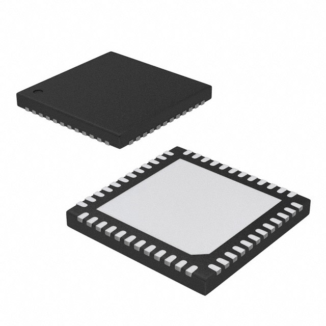
The AD9574 provides a multiple output clock generator function comprising a dedicated phase-locked loop (PLL) core optimized for Ethernet and gigabit Ethernet line card applications. The integer-N PLL design is based on the Analog Devices, Inc., proven portfolio of high performance, low jitter frequency synthesizers to maximize network performance. The AD9574 also benefits other applications requiring low phase noise and jitter performance.Configuring the AD9574 for a particular application requires only the connection of external pull-up or pull-down resistors to the appropriate pin program reader pins (PPRx). These pins provide control of the internal dividers for establishing the desired frequency translations, clock output functionality, and input reference functionality. Connecting an external 19.44 MHz or 25 MHz oscillator to one or both of the REF0_P/REF0_N or REF1_P/REF1_N reference inputs results in a set of output frequencies prescribed by the PPRx pins. Connecting a stable clock source (8 kHz/10 MHz/19.44 MHz/25 MHz/38.88 MHz) to the monitor clock input enables the optional monitor circuit providing quality of service (QoS) status for REF0 or REF1.The PLL section consists of a low noise phase frequency detector (PFD), a precision charge pump (CP), a partially integrated loop filter (LF), a low phase noise voltage controlled oscillator (VCO), and feedback and output dividers. The divider values depend on the PPRx pins. The integrated loop filter requires only a single external capacitor connected to the LF pin.The AD9574 is packaged in a 48-lead 7 mm × 7 mm LFCSP, requiring only a single 3.3 V supply. The operating temperature range is −40°C to +85°C.ApplicationsEthernet line cards, switches, and routersSATA and PCI expressLow jitter, low phase noise clock generation
Technical Specifications
Parameters and characteristics for this part
| Specification | AD9574BCPZ |
|---|---|
| Differential Input | Yes |
| Differential Output | Yes |
| Divider | Yes |
| Frequency - Max | 312.5 MHz |
| Input | Clock |
| Input Ratio | 2 |
| Mounting Type | Surface Mount |
| Multiplier | Yes |
| Number of Circuits | 1 |
| Operating Temperature (Max) | 85 °C |
| Operating Temperature (Min) | -40 °C |
| Output | HCSL, CMOS, HSTL, LVDS |
| Output Ratio | 7 |
| Package / Case | 48-WFQFN Exposed Pad, CSP |
| Package Length | 7 mm |
| Package Name | 48-LFCSP |
| Package Width | 7 mm |
| PLL | Yes with Bypass |
| Voltage - Supply (Maximum) | 3.63 V |
| Voltage - Supply (Minimum) | 2.97 V |
Pricing
Prices provided here are for design reference only. For realtime values and availability, please visit the distributors directly
Sign in to see pricing
Create a free account to access distributor pricing data.
CAD
3D models and CAD resources for this part
Documents
Technical documentation and resources