


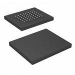
Description
General part information
S29JL032J Series
S29JL032J70BHI310 is a S29JL032J 32Mb (4M × 8Bit/2M × 16Bit), 3V, simultaneous read/write flash memory. Word mode data appears on DQ15–DQ0; byte mode data appears on DQ7–DQ0. The device is designed to be programmed in-system with the standard 3.0 volt VCC supply, and can also be programmed in standard EPROM programmers. Standard control pins—chip enable (CE#), write enable (WE#), and output enable (OE#)—control normal read and write operations, and avoid bus contention issues. The device requires only a single 3.0 volt power supply for both read and write functions. Internally generated and regulated voltages are provided for the program and erase operations.
Technical Specifications
Parameters and characteristics for this part
| Specification | S29JL032J70BHI310 |
|---|---|
| Access Time | 70 ns |
| Memory Depth (Option 1) | 4 M |
| Memory Depth (Option 2) | 2 M |
| Memory Format | FLASH |
| Memory Interface (Type) | Parallel |
| Memory Organization | 2M x 16, 4M x 8 |
| Memory Size | 4 MB |
| Memory Type | Non-Volatile |
| Memory Width (Option 1) | 8 bit |
| Memory Width (Option 2) | 16 bit |
| Mounting Type | Surface Mount |
| Operating Temperature (Max) | 85 °C |
| Operating Temperature (Min) | -40 °C |
| Package / Case | 48-VFBGA |
| Package Length | 8.15 mm |
| Package Name | 48-FBGA |
| Package Width | 6.15 mm |
| Technology | FLASH - NOR |
| Voltage - Supply (Maximum) | 3.6 V |
| Voltage - Supply (Minimum) | 2.7 V |
| Write Cycle Time - Page | 70 ns |
| Write Cycle Time - Word | 70 ns |
Pricing
Prices provided here are for design reference only. For realtime values and availability, please visit the distributors directly
Sign in to see pricing
Create a free account to access distributor pricing data.
CAD
3D models and CAD resources for this part
Documents
Technical documentation and resources

