


ADL5513ACPZ-R7
ActiveLOGARITHMIC DETECTOR, 1 MHZ TO 4 GHZ, -67 TO 8 DBM, 2.7 TO 5.5 V, -40 TO 125 °C, LFCSP-EP-16

ADL5513ACPZ-R7
ActiveLOGARITHMIC DETECTOR, 1 MHZ TO 4 GHZ, -67 TO 8 DBM, 2.7 TO 5.5 V, -40 TO 125 °C, LFCSP-EP-16
Description
General part information
ADL5513 Series
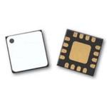
The ADL5513 is a demodulating logarithmic amplifier, capable of accurately converting an RF input signal to a corresponding decibel-scaled output. It employs the progressive compression technique over a cascaded amplifier chain, each stage of which is equipped with a detector cell. The device can be used in either measurement or controller modes. The ADL5513 maintains accurate log conformance for signals up to 4 GHz. The input dynamic range is typically 80 dB (referred to 50 Ω) with error less than ±3 dB and 74 dB with error less than ±1 dB. That dynamic range is held nearly constant over the entire 4 GHz frequency range. The ADL5513 has a 20 ns response time that enables RF burst detection to a pulse rate of beyond 50 MHz. The device provides unprecedented logarithmic intercept stability vs. ambient temperature conditions. A supply voltage of 2.7 V to 5.5 V is required to power the device. Current consumption is 31 mA, and it decreases to 200 μA when the device is disabled.The ADL5513 can be configured to provide a control voltage to a power amplifier or a measurement output from the VOUT pin. Because the output can be used for controller applications, special attention has been paid to minimize wideband noise. In this mode, the setpoint control voltage is applied to the VSET pin. The feedback loop through an RF amplifier is closed via VOUT, the output of which regulates the amplifier output to a magnitude corresponding to VSET. The ADL5513 provides 0 V to (VPOS− 0.1 V) output capability at the VOUT pin, suitable for controller applications. As a measurement device, VOUT is externally connected to VSET to produce an output voltage, VOUT, that increases linear-in-dB with RF input signal amplitude.The logarithmic slope is 21 mV/dB, determined by the VSET interface. The intercept is -88 dBm (referred to 50 Ω, continuous wave input, 900 MHz) using the INHI input. These parameters are very stable against supply and temperature variations.The ADL5513 is fabricated on a SiGe bipolar IC process and is available in a 3 mm × 3 mm, 16-lead LFCSP package for the −40°C to +125°C operating temperature range. A fully populated evaluation board is available.ApplicationsRF transmitter power amplifier linearization and gain/power controlPower monitoring in radio link transmittersRSSI measurement in base stations, WLAN, WiMAX, RADAR
Technical Specifications
Parameters and characteristics for this part
| Specification | ADL5513ACPZ-R7 |
|---|---|
| Accuracy | 0.5 dB |
| Current - Supply | 31 mA |
| Frequency (Max) | 4 GHz |
| Frequency (Min) | 1 MHz |
| Input Level (Max) | 6 dBm |
| Input Level (Min) | -58 dBm |
| Mounting Type | Surface Mount |
| Package / Case | 16-VFQFN Exposed Pad, CSP |
| Package Length | 3 mm |
| Package Name | 16-LFCSP-VQ |
| Package Width | 3 mm |
| RF Type | WLAN, WiMAX |
| Voltage - Supply (Maximum) | 5.5 V |
| Voltage - Supply (Minimum) | 2.7 V |
Pricing
Prices provided here are for design reference only. For realtime values and availability, please visit the distributors directly
Sign in to see pricing
Create a free account to access distributor pricing data.
CAD
3D models and CAD resources for this part
Documents
Technical documentation and resources