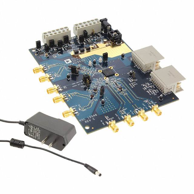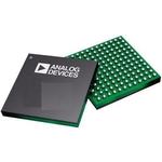
AD9652BBCZ-310
Active2-CHANNEL DUAL ADC PIPELINED 310MSPS 16-BIT PARALLEL 144-PIN CSP-BGA TRAY
AD9652BBCZ-310
Active2-CHANNEL DUAL ADC PIPELINED 310MSPS 16-BIT PARALLEL 144-PIN CSP-BGA TRAY
Description
General part information
AD9652 Series
The AD9652 is a dual, 16-bit analog-to-digital converter (ADC) with sampling speeds of up to 310 MSPS. It is designed to support demanding, high speed signal processing applications that require exceptional dynamic range over a wide input frequency range (up to 465 MHz). Its exceptional low noise floor of −157.6 dBFS and large signal spurious-free dynamic range (SFDR) performance (exceeding 85 dBFS, typical) allows low level signals to be resolved in the presence of large signals.The dual ADC cores feature a multistage, pipelined architecture with integrated output error correction logic. A high performance on-chip buffer and internal voltage reference simplify the inter-face to external driving circuitry while preserving the exceptional performance of the ADC.The AD9652 can support input clock frequencies of up to 1.24 GHz with a 1, 2, 4, and 8 integer clock divider used to generate the ADC sample clock. A duty cycle stabilizer is provided to compensate for variations in the ADC clock duty cycle. The 16-bit output data (with an overrange bit) from each ADC is interleaved onto a single LVDS output port along with a double data rate (DDR) clock. Programming for setup and control are accomplished using a 3-wire SPI-compatible serial interface.The AD9652 is available in a 144-ball CSP_BGA and is specified over the industrial temperature range of −40°C to +85°C. This product is protected by pending U.S. patents.PRODUCT HIGHLIGHTSIntegrated dual, 16-bit, 310 MSPS ADCs.On-chip buffer simplifies ADC driver interface.Operation from a 3.3 V and 1.8 V supply and a separate digital output driver supply accommodating LVDS outputs.Proprietary differential input maintains excellent SNR performance for input frequencies of up to 485 MHz.SYNC input allows synchronization of multiple devices.Three-wire, 3.3 V or 1.8 V SPI port for register programming and readback.APPLICATIONSMiltary radar and communicationsMultimode digital receivers (3G or 4G)Test and InstrumentationSmart antenna systems
Technical Specifications
Parameters and characteristics for this part
| Specification | AD9652BBCZ-310 |
|---|---|
| Architecture | Pipelined |
| Configuration | S/H-ADC |
| Data Interface | LVDS - Parallel |
| Features | Simultaneous Sampling |
| Input Type | Differential |
| Mounting Type | Surface Mount |
| Number of A/D Converters | 2 count |
| Number of Bits | 16 bits |
| Number of Inputs | 2 |
| Operating Temperature (Max) | 85 °C |
| Operating Temperature (Min) | -40 °C |
| Package / Case | CSPBGA, 144-LFBGA |
| Package Length | 10 mm |
| Package Name | 144-CSPBGA |
| Package Width | 10 mm |
| Ratio - ADC | 1 |
| Ratio - S/H | 1 |
| Reference Type | External, Internal |
| Sampling Rate (Per Second) | 310 MHz |
| Voltage - Supply, Analog | 3.3V, 1.8V |
| Voltage - Supply, Analog | 3.3 V, 1.8 V |
| Voltage - Supply, Digital (Max) | 1.9 V |
| Voltage - Supply, Digital (Min) | 1.7 V |
Pricing
Prices provided here are for design reference only. For realtime values and availability, please visit the distributors directly
Sign in to see pricing
Create a free account to access distributor pricing data.
CAD
3D models and CAD resources for this part
Documents
Technical documentation and resources