


ADP1196 Series
5 V, 3 A Logic Controlled High-Side or Low-Side Load Switch
Manufacturer: Analog Devices Inc./Maxim Integrated
Catalog
5 V, 3 A Logic Controlled High-Side or Low-Side Load Switch
Description
AI
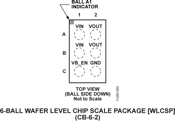
The ADP1196 is a high-side or low-side load switch designed for VIN operation between 0 V and 5.5 V with a VB_EN supply of 1.83 V to 5.5 V. The device contains an internal charge pump that operates from either VIN or VB_EN, whichever is higher, and an ultralow on resistance, N-channel MOSFET. This N-channel MOSFET supports more than 2 A of continuous current at VIN close to 0 V, and, with its ultralow on resistance, minimizes power loss. In addition, the on resistance is constant, independent of the VIN or VB_EN voltage. The low 26 μA quiescent current and ultralow shutdown current make the ADP1196 ideal for low power applications.When the junction temperature exceeds 125°C, overtemperature protection circuitry is activated, thereby protecting the ADP1196 and downstream circuits from potential damage.The ADP1196 occupies minimal printed circuit board (PCB) space, with an area of less than 1.5 mm2and a height of 0.60 mm.The ADP1196 is available in an ultrasmall 1.0 mm × 1.5 mm, 6-ball, 0.5 mm pitch WLCSP.APPLICATIONSCommunications and InfrastructureTEC Controller reverse polarity for Heating/CoolingFine Line Geometry Core Voltage In-rush current controlMedical and HealthcareInstrumentation

