LTC2215IUP#PBF
Active16-BIT, 65MSPS LOW NOISE ADC
Deep-Dive with AI
Search across all available documentation for this part.
LTC2215IUP#PBF
Active16-BIT, 65MSPS LOW NOISE ADC
Deep-Dive with AI
Technical Specifications
Parameters and characteristics for this part
| Specification | LTC2215IUP#PBF |
|---|---|
| Architecture | Pipelined |
| Configuration | S/H-ADC |
| Data Interface | LVDS - Parallel, Parallel |
| Features | PGA |
| Input Type | Differential |
| Mounting Type | Surface Mount |
| Number of A/D Converters | 1 |
| Number of Bits | 16 |
| Number of Inputs | 1 |
| Operating Temperature [Max] | 85 °C |
| Operating Temperature [Min] | -40 °C |
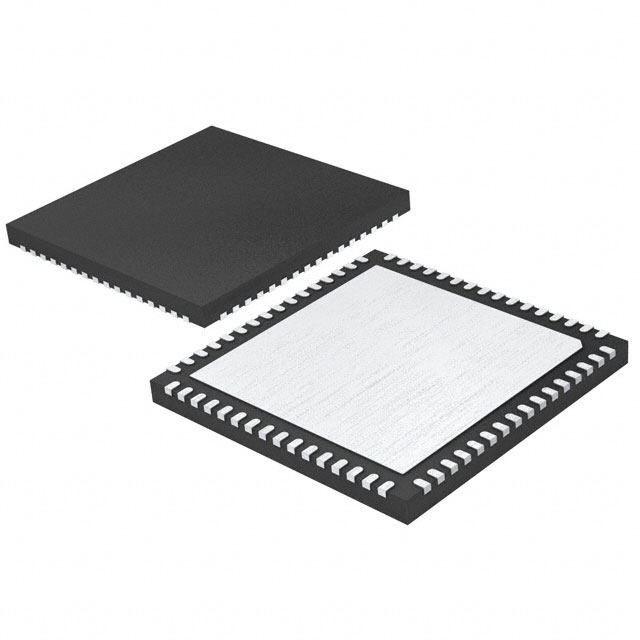
| Package / Case | 64-WFQFN Exposed Pad |
| Ratio - S/H:ADC | 1:1 |
| Reference Type | External, Internal |
| Sampling Rate (Per Second) | 65 M |
| Supplier Device Package | 64-QFN (9x9) |
| Voltage - Supply, Analog [Max] | 3.465 V |
| Voltage - Supply, Analog [Min] | 3.135 V |
| Voltage - Supply, Digital [Max] | 3.465 V |
| Voltage - Supply, Digital [Min] | 3.135 V |
Pricing
Prices provided here are for design reference only. For realtime values and availability, please visit the distributors directly
| Distributor | Package | Quantity | $ | |
|---|---|---|---|---|
| Digikey | Tube | 1 | $ 129.04 | |
| 10 | $ 105.32 | |||
| 25 | $ 100.31 | |||
Description
General part information
LTC2215 Series
The LTC2216/LTC2215 are 80Msps/65Msps sampling 16- bit A/D converters designed for digitizing high frequency, wide dynamic range signals with input frequencies up to 400MHz. The input range of the ADC is fixed at 2.75VP-P.The LTC2216/LTC2215 are perfect for demanding communications applications, with AC performance that includes 81.5dBFS noise floor and 100dB spurious free dynamic range (SFDR). Ultra low jitter of 85fsRMSallows undersampling of high input frequencies while maintaining excellent noise performance. Maximum DC specs include ±3.5LSB INL, ±1LSB DNL (no missing codes).The digital output can be either differential LVDS or single-ended CMOS. There are two format options for the CMOS outputs: a single bus running at the full data rate or demultiplexed buses running at half data rate. A separate output power supply allows the CMOS output swing to range from 0.5V to 3.6V.The ENC+and ENC–inputs may be driven differentially or single-ended with a sine wave, PECL, LVDS, TTL or CMOS inputs. An optional clock duty cycle stabilizer allows high performance at full speed with a wide range of clock duty cycles.ApplicationsTelecommunicationsReceiversCellular Base StationsSpectrum AnalysisImaging SystemsATE
Documents
Technical documentation and resources