LTC2164IUK#TRPBF
Active16-BIT, 105MSPS LOW POWER ADCS
Deep-Dive with AI
Search across all available documentation for this part.
LTC2164IUK#TRPBF
Active16-BIT, 105MSPS LOW POWER ADCS
Deep-Dive with AI
Technical Specifications
Parameters and characteristics for this part
| Specification | LTC2164IUK#TRPBF |
|---|---|
| Architecture | Pipelined |
| Configuration | S/H-ADC |
| Data Interface | LVDS - Parallel, Parallel |
| Input Type | Differential |
| Mounting Type | Surface Mount |
| Number of A/D Converters | 1 |
| Number of Bits | 16 |
| Number of Inputs | 1 |
| Operating Temperature [Max] | 85 °C |
| Operating Temperature [Min] | -40 °C |
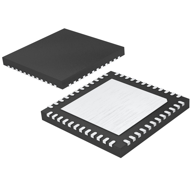
| Package / Case | 48-WFQFN Exposed Pad |
| Ratio - S/H:ADC | 1:1 |
| Reference Type | External, Internal |
| Sampling Rate (Per Second) | 105 M |
| Supplier Device Package | 48-QFN (7x7) |
| Voltage - Supply, Analog [Max] | 1.9 V |
| Voltage - Supply, Analog [Min] | 1.7 V |
| Voltage - Supply, Digital [Max] | 1.9 V |
| Voltage - Supply, Digital [Min] | 1.7 V |
Pricing
Prices provided here are for design reference only. For realtime values and availability, please visit the distributors directly
| Distributor | Package | Quantity | $ | |
|---|---|---|---|---|
| Digikey | Cut Tape (CT) | 1 | $ 128.25 | |
| Digi-Reel® | 1 | $ 128.25 | ||
| Tape & Reel (TR) | 2000 | $ 99.60 | ||
Description
General part information
LTC2164 Series
The LTC2165/LTC2164/LTC2163 are sampling 16-bit A/D converters designed for digitizing high frequency, wide dynamic range signals. They are perfect for demanding communications applications with AC performance that includes 76.8dB SNR and 90dB spurious free dynamic range (SFDR). Ultralow jitter of 0.07psRMSallows undersampling of IF frequencies with excellent noise performance.DC specs include ±2LSB INL (typ), ±0.5LSB DNL (typ) and no missing codes over temperature. The transition noise is 3.4LSBRMS.The digital outputs can be either full rate CMOS, double data rate CMOS, or double data rate LVDS. A separate output power supply allows the CMOS output swing to range from 1.2V to 1.8V.The ENC+and ENC–inputs may be driven differentially or single-ended with a sine wave, PECL, LVDS, TTL, or CMOS inputs. An optional clock duty cycle stabilizer allows high performance at full speed for a wide range of clock duty cycles.ApplicationsCommunicationsCellular Base StationsSoftware Defined RadiosPortable Medical ImagingMultichannel Data AcquisitionNondestructive Testing
Documents
Technical documentation and resources