


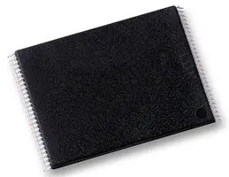
MT29F1G08ABAEAWP:E
LTBFLASH MEMORY, SLC NAND, 1 GBIT, 128M X 8BIT, PARALLEL, TSOP-I, 48 PINS

MT29F1G08ABAEAWP:E
LTBFLASH MEMORY, SLC NAND, 1 GBIT, 128M X 8BIT, PARALLEL, TSOP-I, 48 PINS
Description
General part information
MT29F1G08ABAEAWP:E
MT29F1G08ABAEAWP:E is a NAND flash device that includes an asynchronous data interface for high-performance I/O operations. This device uses a highly multiplexed 8-bit bus (I/Ox) to transfer commands, addresses, and data. There are five control signals used to implement the asynchronous data interface: CE#, CLE, ALE, WE#, and RE#. Additional signals control hardware write protection and monitor device status (R/B#). This hardware interface creates a low pin-count device with a standard pinout that remains the same from one density to another, enabling future upgrades to higher densities with no board redesign. A target is the unit of memory accessed by a chip-enabled signal. A target contains one or more NAND Flash die. A NAND Flash die is the minimum unit that can independently execute commands and report status.
Technical Specifications
Parameters and characteristics for this part
| Specification | MT29F1G08ABAEAWP:E |
|---|---|
| Memory Depth | 128 M |
| Memory Format | FLASH |
| Memory Interface (Type) | Parallel |
| Memory Size | 1 Gbit |
| Memory Type | Non-Volatile |
| Memory Width | 8 bit |
| Mounting Type | Surface Mount |
| Operating Temperature (Max) | 70 °C |
| Operating Temperature (Min) | 0 °C |
| Package Length | 0.724 " |
| Package Name | 48-TFSOP, 48-TSOP I |
| Package Width | 18.4 mm |
| Technology | FLASH - NAND |
| Voltage - Supply (Maximum) | 3.6 V |
| Voltage - Supply (Minimum) | 2.7 V |
Pricing
Prices provided here are for design reference only. For realtime values and availability, please visit the distributors directly
Sign in to see pricing
Create a free account to access distributor pricing data.
CAD
3D models and CAD resources for this part
Documents
Technical documentation and resources
No documents available