


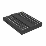
MT41K512M8DA-093:P
LTBDRAM, DDR3L, 4 GBIT, 512M X 8BIT, 1.066 GHZ, TFBGA, 78 PINS

MT41K512M8DA-093:P
LTBDRAM, DDR3L, 4 GBIT, 512M X 8BIT, 1.066 GHZ, TFBGA, 78 PINS
Description
General part information
MT41K512M8DA-093:P
MT41K512M8DA-093:P is a DDR3L SDRAM (1.35V). The double data rate architecture is an 8n-prefetch architecture with an interface designed to transfer two data words per clock cycle at the I/O pins. A single read or write operation for the DDR3 SDRAM effectively consists of a single 8n-bit-wide, four-clock cycle data transfer at the internal DRAM core and eight corresponding n-bit-wide, one-half-clock-cycle data transfers at the I/O pins. The differential data strobe (DQS, DQS#) is transmitted externally, along with data, for use in data capture at the DDR3 SDRAM input receiver. DQS is center-aligned with data for WRITEs. The read data is transmitted by the DDR3 SDRAM and edge-aligned to the data strobes. The DDR3 SDRAM operates from a differential clock (CK and CK#).
Technical Specifications
Parameters and characteristics for this part
| Specification | MT41K512M8DA-093:P |
|---|---|
| Access Time | 20 ns |
| Clock Frequency | 1.066 GHz |
| Memory Depth | 512 M |
| Memory Format | DRAM |
| Memory Interface (Type) | Parallel |
| Memory Size | 4 Gbit |
| Memory Type | Volatile |
| Memory Width | 8 bit |
| Mounting Type | Surface Mount |
| Operating Temperature (Max) | 95 °C |
| Operating Temperature (Min) | 0 °C |
| Package / Case | 78-TFBGA |
| Package Length | 8 mm |
| Package Name | 78-FBGA |
| Package Width | 10.5 mm |
| Technology | SDRAM - DDR3L |
| Voltage - Supply (Maximum) | 1.45 V |
| Voltage - Supply (Minimum) | 1.283 V |
Pricing
Prices provided here are for design reference only. For realtime values and availability, please visit the distributors directly
Sign in to see pricing
Create a free account to access distributor pricing data.
CAD
3D models and CAD resources for this part
Documents
Technical documentation and resources