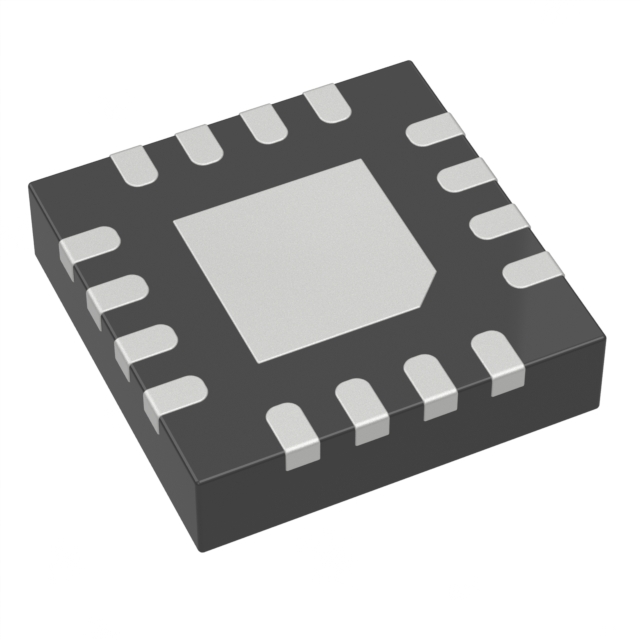
SY89871UMG
ActiveCLOCK BUFFER, DIVIDER, FANOUT 3.2 GHZ TO 2 OUTPUTS, 2.375 V TO 3.63 V, 16 PINS, QFN-EP
Deep-Dive with AI
Search across all available documentation for this part.

SY89871UMG
ActiveCLOCK BUFFER, DIVIDER, FANOUT 3.2 GHZ TO 2 OUTPUTS, 2.375 V TO 3.63 V, 16 PINS, QFN-EP
Deep-Dive with AI
Technical Specifications
Parameters and characteristics commom to parts in this series
| Specification | SY89871UMG | SY89871 Series |
|---|---|---|
| Differential - Input:Output | - | True |
| Differential - Input:Output | - | True |
| Frequency - Max | - | 2.5 GHz |
| Input | - | LVPECL, HSTL, CML, LVDS |
| Mounting Type | - | Surface Mount |
| null | - | |
| Number of Circuits | - | 1 |
| Operating Temperature | - | 85 °C |
| Operating Temperature | - | -40 °C |
| Output | - | LVPECL |
| Package / Case | - | 16-MLF®, 16-VFQFN Exposed Pad |
| Ratio - Input:Output | - | 1:3 |
| Type | - | Divider, Fanout Buffer (Distribution) |
| Voltage - Supply | - | 3.63 V |
| Voltage - Supply | - | 2.375 V |
Pricing
Prices provided here are for design reference only. For realtime values and availability, please visit the distributors directly
| Distributor | Package | Quantity | $ | |
|---|---|---|---|---|
| Digikey | Tube | 1 | $ 13.40 | |
| 25 | $ 11.15 | |||
| 100 | $ 10.15 | |||
| Microchip Direct | TUBE | 1 | $ 13.40 | |
| 25 | $ 11.15 | |||
| 100 | $ 10.15 | |||
| 1000 | $ 8.46 | |||
| 5000 | $ 7.81 | |||
| 10000 | $ 7.26 | |||
SY89871 Series
IC CLK BUFFER 1:3 2.5GHZ 16MLF
| Part | Voltage - Supply [Max] | Voltage - Supply [Min] | Mounting Type | Differential - Input:Output [custom] | Differential - Input:Output [custom] | Package / Case | Operating Temperature [Max] | Operating Temperature [Min] | Ratio - Input:Output [custom] | Frequency - Max [Max] | Type | Number of Circuits | Output | Input |
|---|---|---|---|---|---|---|---|---|---|---|---|---|---|---|
Microchip Technology SY89871UMI-TR | 3.63 V | 2.375 V | Surface Mount | 16-MLF®, 16-VFQFN Exposed Pad | 85 °C | -40 °C | 1:3 | 2.5 GHz | Divider, Fanout Buffer (Distribution) | 1 | LVPECL | CML, HSTL, LVDS, LVPECL | ||
Microchip Technology SY89871UMG | ||||||||||||||
Microchip Technology SY89871UMG-TR | 3.63 V | 2.375 V | Surface Mount | 16-MLF®, 16-VFQFN Exposed Pad | 85 °C | -40 °C | 1:3 | 2.5 GHz | Divider, Fanout Buffer (Distribution) | 1 | LVPECL | CML, HSTL, LVDS, LVPECL | ||
Microchip Technology SY89871UMG | 3.63 V | 2.375 V | Surface Mount | 16-MLF®, 16-VFQFN Exposed Pad | 85 °C | -40 °C | 1:3 | 2.5 GHz | Divider, Fanout Buffer (Distribution) | 1 | LVPECL | CML, HSTL, LVDS, LVPECL | ||
Microchip Technology SY89871UMI | 3.63 V | 2.375 V | Surface Mount | 16-MLF®, 16-VFQFN Exposed Pad | 85 °C | -40 °C | 1:3 | 2.5 GHz | Divider, Fanout Buffer (Distribution) | 1 | LVPECL | CML, HSTL, LVDS, LVPECL |
Description
General part information
SY89871 Series
The SY89871U is a 2.5V/3.3V LVPECL output precision clock divider capable of accepting a high-speed differential clock input (AC or DC-coupled) CML, LVPECL, HSTL or LVDS clock input signal and dividing down the frequency using a programmable divider ratio to create a frequencylocked lower speed version of the input clock (Bank B). Available divider ratios are 2, 4, 8, and 16. In a typical 622MHz clock system this would provide availability of 311MHz, 115MHz, 77MHz, or 38MHz auxiliary clock components. The differential input buffer has a unique internal termination design that allows access to the termination network through a VT pin. This feature allows the device to easily interface to different logic standards. A VREF-AC reference is included for AC-coupled applications. The SY89871U includes two phase-matched output banks. Bank A (QA) is a frequency-matched copy of the input. Bank B (QB0, QB1) is a divided down output of the input frequency. Bank A and Bank B maintain a matched delay independent of the divider setting.Two matched-delay outputs: - Bank A: undivided pass-through (QA) - Bank B: programmable divide by 2, 4, 8, 16 (QB0, QB1) Matched delay: all outputs have matched delay, independent of divider setting Guaranteed AC performance: >2.5GHz fMAX <250ps tr /tf <670ps tpd (matched delay) <15ps within-device skew Low jitter design - 231fs RMS phase jitter (Typ) Power supply 3.3V or 2.5V Unique patent-pending input termination and VT pin for DC- and AC- coupled inputs: any differential inputs (LVPECL, LVDS, CML, HSTL) TTL/CMOS inputs for select and reset 100K EP compatible LVPECL outputs Parallel programming capability Wide operating temperature range: -40°C to +85°C Available in 16-pin (3mm x 3mm) QFN package
Documents
Technical documentation and resources


