


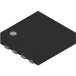

Description
General part information
S25FS256SAGNFI001
S25FS256SAGNFI001 is a FS-S flash non-volatile memory using MIRRORBIT™ technology - that stores two data bits in each memory array transistor, eclipse architecture - that dramatically improves program and erase performance, 65-nm process lithography. The S25FS-S family connects to a host system via a serial peripheral interface (SPI). This multiple width interface is called SPI multi-I/O or MIO. In addition, this is double data rate (DDR) read commands for QIO and QPI that transfer address and read data on both edges of the clock. The FS-S Eclipse architecture features a page programming buffer that allows up to 512bytes to be programmed in one operation, resulting in faster effective programming and erase than prior generation SPI program or erase algorithms.
Technical Specifications
Parameters and characteristics for this part
| Specification | S25FS256SAGNFI001 |
|---|---|
| Clock Frequency | 133 MHz |
| Memory Depth | 32 M |
| Memory Format | FLASH |
| Memory Interface (Type) | QPI, SPI - Quad I/O |
| Memory Size | 256 Mbit |
| Memory Type | Non-Volatile |
| Memory Width | 8 bit |
| Mounting Type | Surface Mount |
| Operating Temperature (Max) | 85 °C |
| Operating Temperature (Min) | -40 °C |
| Package / Case | 8-WDFN Exposed Pad |
| Package Length | 6 |
| Package Name | 8-WSON |
| Package Width | 8 |
| Technology | FLASH - NOR |
| Voltage - Supply (Maximum) | 2 V |
| Voltage - Supply (Minimum) | 1.7 V |
Pricing
Prices provided here are for design reference only. For realtime values and availability, please visit the distributors directly
Sign in to see pricing
Create a free account to access distributor pricing data.
CAD
3D models and CAD resources for this part
Documents
Technical documentation and resources