


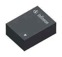

Description
General part information
BGSX22G5A10E6327XTSA1
The BGSX22G5A10 RF MOS switch is specifically designed for LTE and WCDMA multi antenna applications. This DPDT offers low insertion loss and low harmonic generation paired with high isolation between RF ports. The switch is controlled via a GPIO interface. The on-chip controller allows power-supply voltages from 1.65V to 3.4V. The switch features direct-connect-to-battery functionality and DC-free RF ports. Unlike GaAs technology, external DC blocking capacitors at the RF Ports are only required if DC voltage is applied externally. The BGSX22G5A10 RF Switch is manufactured in Infineon’s patented MOS technology, offering the performance of GaAs with the economy and integration of conventional CMOS including the inherent higher ESD robustness. The device has a very small size of only 1.1 x 1.5mm2and a maximum thickness of 0.55 mm.
Technical Specifications
Parameters and characteristics for this part
| Specification | BGSX22G5A10E6327XTSA1 |
|---|---|
| Circuit | DPDT |
| Frequency Range (Max) | 6 GHz |
| Frequency Range (Min) | 100 MHz |
| IIP3 | 80 dBm |
| Impedance | 50 Ohm |
| Insertion Loss | 1.1 dB |
| Isolation | 38 dB |
| Mounting Type | Surface Mount |
| Operating Temperature (Max) | 85 °C |
| Operating Temperature (Min) | -40 °C |
| Package / Case | 10-UFQFN |
| Package Name | PG-ATSLP-10-50 |
| RF Type | LTE, W-CDMA |
| Test Frequency (Maximum) | 5.925 GHz |
| Test Frequency (Minimum) | 5.15 GHz |
| Voltage - Supply (Maximum) | 3.4 V |
| Voltage - Supply (Minimum) | 1.65 V |
Pricing
Prices provided here are for design reference only. For realtime values and availability, please visit the distributors directly
Sign in to see pricing
Create a free account to access distributor pricing data.
CAD
3D models and CAD resources for this part
Documents
Technical documentation and resources