


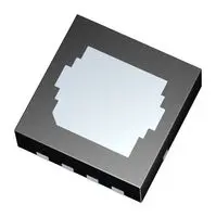

Description
General part information
IQE030N06NM5CGSCATMA1
Infineon is presenting the new product of the portfolio extension for the innovativeSource-Downtechnology: theOptiMOSTM5 60 VPQFN 3.3x3.3 Source-Down: IQE030N06NM5CGSC. The revolutionary Source-Down technology introduces a flipped silicon die, which is positioned upside down inside of the components. This adjustment allows the source potential (instead of the drain potential) to be connected to the PCB over the thermal pad. Therefore, it offers several advantages, such as increased thermal capability, advanced power density or improved layout possibilities. Furthermore, the higher efficiency, the reduced active cooling requirements and the effective layout for thermal management are benefits at the system level. Thanks to the new benchmark RDS(on)and the innovative layout capacities enable the Source-Down concept to have a leading position in temperature management. Moreover, with the dual-side cooling package three times more power can be dissipated compared to the overmolded package. The Source-Down portfolio is addressing applications, such as drives, telecom, SMPS or server. The new technology can be found in two different footprints for now: Source-Down Standard-Gate and Source-Down Center-Gate (optimized for parallelization).
Technical Specifications
Parameters and characteristics for this part
| Specification | IQE030N06NM5CGSCATMA1 |
|---|---|
| Current - Continuous Drain (Id) (Ta) | 21 A |
| Current - Continuous Drain (Id) (Tc) | 132 A |
| Drain to Source Voltage (Vdss) | 60 V |
| Drive Voltage (Max Rds On) | 6 V |
| Drive Voltage (Min Rds On) | 10 V |
| FET Type | N-Channel |
| Gate Charge (Max) | 49 nC, 49 nC |
| Input Capacitance (Ciss) (Max) | 3800 pF |
| Mounting Type | Surface Mount |
| Operating Temperature (Max) | 175 °C |
| Operating Temperature (Min) | -55 °C |
| Package / Case | 9-PowerWDFN |
| Package Name | PG-WHTFN-9-1 |
| Power Dissipation (Max) | 2.5 W, 100 W |
| Rds On (Max) | 3 mOhm |
| Technology | MOSFET (Metal Oxide) |
| Vgs (Max) | 20 V |
| Vgs(th) (Max) | 3.3 V |
Pricing
Prices provided here are for design reference only. For realtime values and availability, please visit the distributors directly
Sign in to see pricing
Create a free account to access distributor pricing data.
CAD
3D models and CAD resources for this part
Documents
Technical documentation and resources