


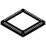
NB3N401SMNTXG
ActiveLVDS DRIVER, DIFFERENTIAL LINE DRIVER / RECEIVER, -40 °C, 85 °C, 3 V, 3.6 V, QFN

NB3N401SMNTXG
ActiveLVDS DRIVER, DIFFERENTIAL LINE DRIVER / RECEIVER, -40 °C, 85 °C, 3 V, 3.6 V, QFN
Description
General part information
NB3N401SMNTXG
The NB3N401S is a 3.3 V supply Quad Multipoint Low Voltage Differential Signals (M−LVDS) line drivers and receivers. The device is TIA/EIA−899 compliant. The device offers the Type 1 receiver threshold at 0.0 V and the Type 2 receiver threshold at 0.1 V. The NB3N401S supports four independent Half Duplex bus configurations. Each of the four sections has Pin (SEL) for selection of Type−1 and Type−2 receivers that detect the bus state with as little as 50 mV of differential input voltage over a common mode voltage range of −1 V to 3.4 V. The Type−1 receivers have near zero thresholds (±50 mV)and exhibit 25 mV of differential input voltage hysteresis to prevent output oscillations with slowly changing signals or loss of input. Type−2 receivers include an offset threshold to provide a detectable voltage under open-circuit, idle-bus, and other faults conditions. The NB3N401S is offered in a 48 Pin 7 mm x 7 mm x 0.9 mm QFN package.
Technical Specifications
Parameters and characteristics for this part
| Specification | NB3N401SMNTXG |
|---|---|
| Data Rate | 250 MHz |
| Duplex | Half |
| Mounting Type | Surface Mount |
| Number of Drivers | 4 |
| Number of Receivers | 4 |
| Operating Temperature (Max) | 85 °C |
| Operating Temperature (Min) | -40 °C |
| Package / Case | 48-VFQFN Exposed Pad |
| Package Length | 7 mm |
| Package Name | 48-QFN |
| Package Width | 7 mm |
| Protocol | LVDS |
| Receiver Hysteresis | 25 mV |
| Type | Transceiver |
| Voltage - Supply (Maximum) | 3.6 V |
| Voltage - Supply (Minimum) | 3 V |
Pricing
Prices provided here are for design reference only. For realtime values and availability, please visit the distributors directly
Sign in to see pricing
Create a free account to access distributor pricing data.
CAD
3D models and CAD resources for this part
Documents
Technical documentation and resources